Plasma processing system, plasma processing method, plasma film deposition system, and plasma film deposition method

a plasma processing system and plasma technology, applied in the field of plasma processing system, plasma processing method, plasma film deposition system, plasma film deposition method, can solve the problems of difficult to generate uniform plasma, lowering efficiency, overheating or causing particles by etching action, etc., to suppress the effect of device destruction of the substrate due to the charging

Inactive Publication Date: 2005-09-15
MITSUBISHI HEAVY IND LTD
View PDF13 Cites 10 Cited by
  • Summary
  • Abstract
  • Description
  • Claims
  • Application Information

AI Technical Summary

Benefits of technology

[0039] As a result, the substrate can be located in a region where the electron temperature is low even though the electron density is

Problems solved by technology

When the lines of magnetic force (lines of magnetic flux density) passed through the wall (tubular surface) of the tubular container, electrons and ions moved along the lines of magnetic force, so that the electrons and ions impinged on the wall of the tubular container, thus posing the possibility of overheating or causing the occurrence of particles by an etching action.
In this case, it has become difficult to generate a uniform plasma over a wide range relative to the

Method used


Image

  • Plasma processing system, plasma processing method, plasma film deposition system, and plasma film deposition method
  • Plasma processing system, plasma processing method, plasma film deposition system, and plasma film deposition method
  • Plasma processing system, plasma processing method, plasma film deposition system, and plasma film deposition method

Examples


second embodiment

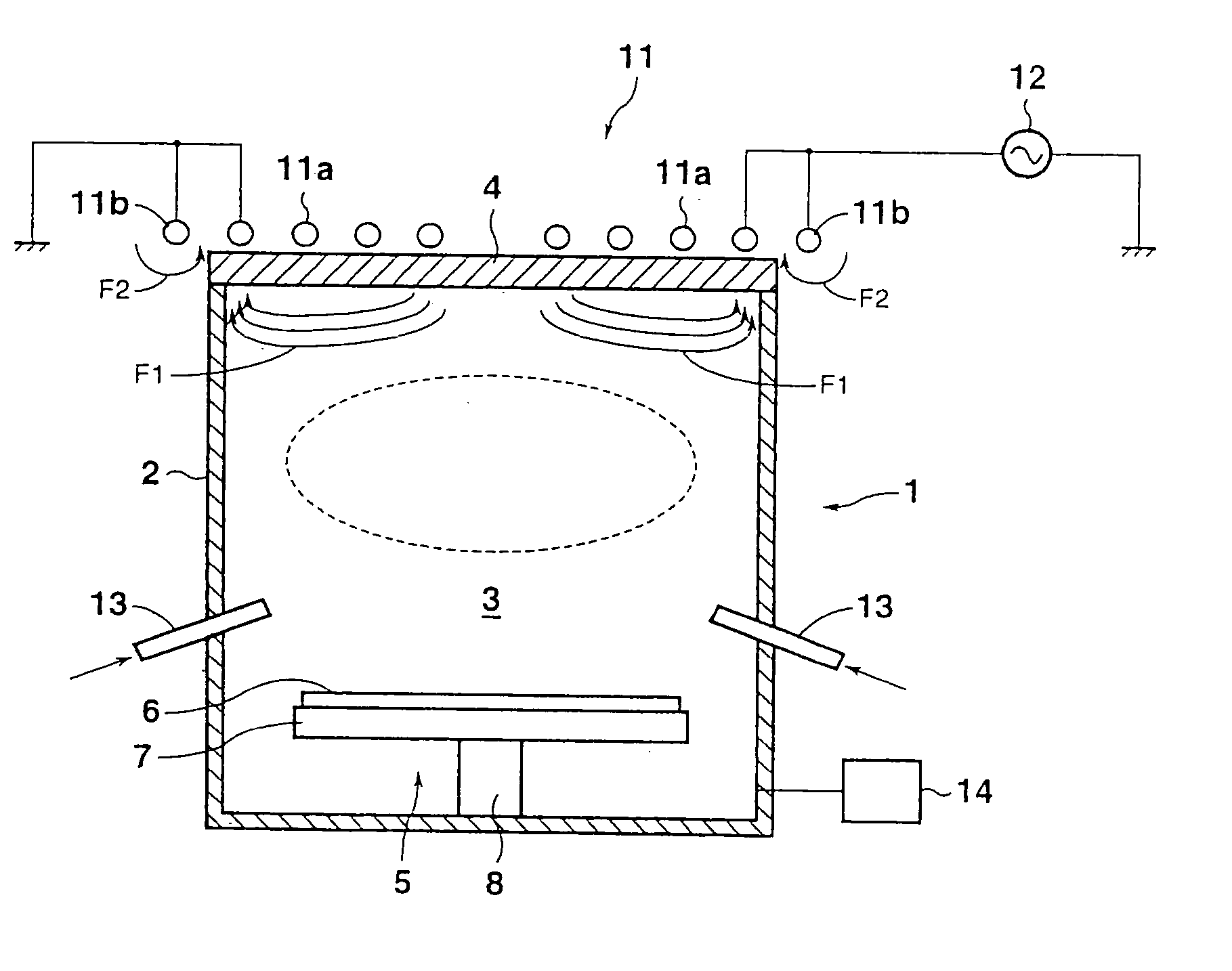
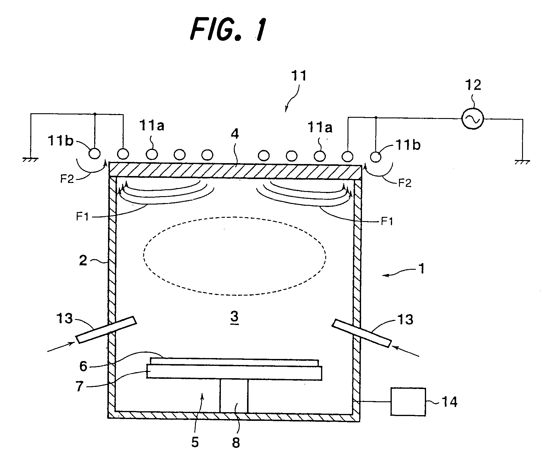
[0079] A second embodiment will be described based on FIG. 3.

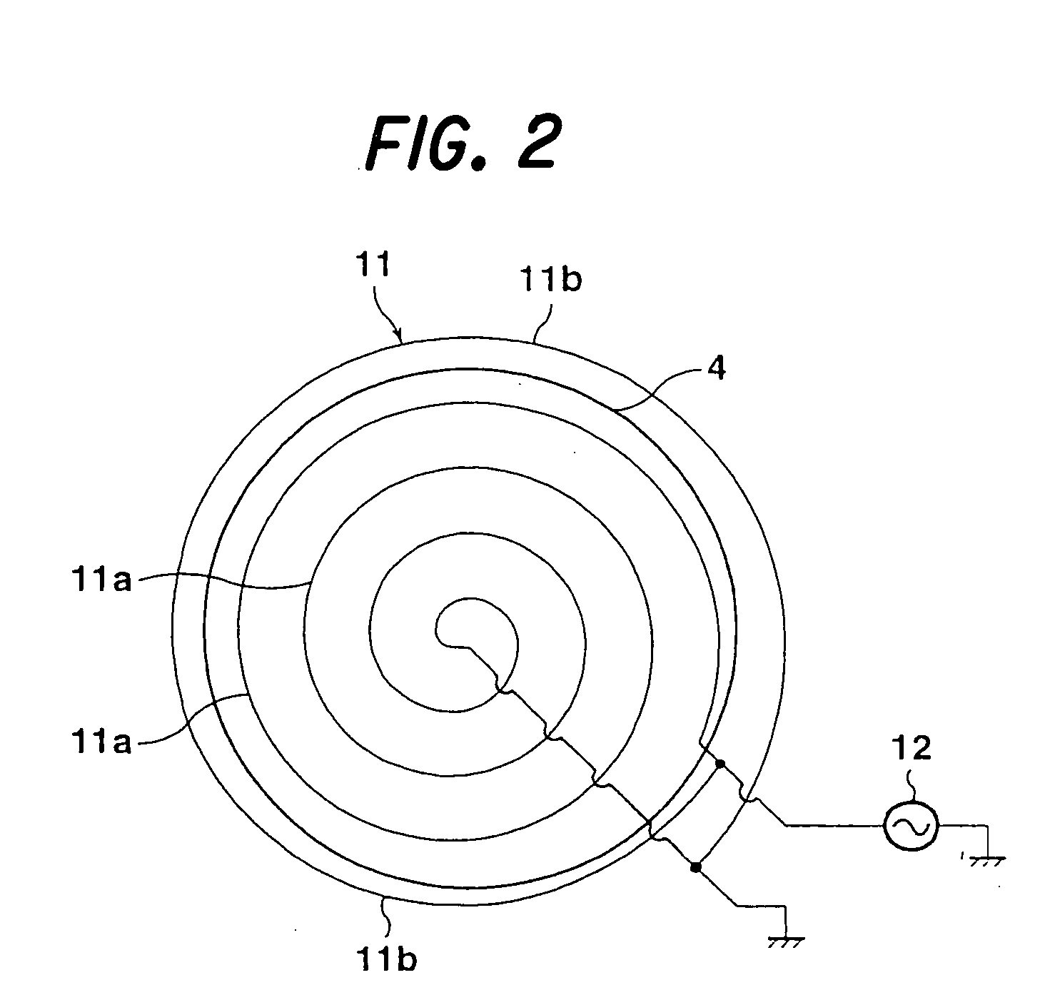
[0080] In the embodiment shown in FIG. 3, a high frequency antenna 11, as an antenna, is the same as that in FIGS. 1 and 2 in terms of its feature, and is in the form of a flat coil. A high frequency power source 12 is connected to the site of the antenna 11a, while a second high frequency power source 21 as second power supply means is connected to the site of a second antenna 11b. An electric current is supplied from the second high frequency power source 21 to the site of the second antenna 11b in a state of connection opposite to that for the site of the antenna 11a. In detail, at the site of the second antenna 11b, the high frequency power source 12 is connected to the coil on the grounded side at the site of the antenna 11a, so that the coil at the site of the antenna 11a on a side, where the high frequency power source 12 is connected, is brought into a grounded state.

[0081] Because of the above-described feature, ...

third embodiment

[0083] A third embodiment will be described based on FIG. 4.

[0084] In the embodiment shown in FIG. 4, a flat coil-shaped high frequency antenna 22, as an antenna having nearly the same diameter as the diameter of a ceiling plate 4, is disposed. A second antenna 23, having a different feature from that of the high frequency antenna 22, is disposed outside of the high frequency antenna 22, namely, outwardly of the ceiling surface. A high frequency power source 12 is connected to the high frequency antenna 22, while a second high frequency power source 24 as second power supply means is connected to the second antenna 23. The high frequency antenna 22 and the second high frequency power source 24 are connected to the high frequency power source 12 and the second high frequency power source 24 in the same direction. The second high frequency power source 24 is connected to the second antenna 23 via a phase shifter 25 as phase changing means.

[0085] An electric current of a phase opposit...

fourth embodiment

[0087] A fourth embodiment will be described based on FIG. 5.

[0088] In the embodiment shown in FIG. 5, a high frequency antenna 31, which has nearly the same diameter as the diameter of a ceiling plate 4, is composed of antennas 31a, 31b, 31c and 31d each in the form of a concentric ring. A ring-shaped second antenna 32 is disposed outside of the high frequency antenna 31, namely, outwardly of the ceiling surface. A high frequency power source 12 is connected in parallel to the antennas 31a, 31b, 31c, 31d, and the second antenna 32 is connected to the high frequency power source 12 in a state of connection opposite to that for the ring antenna 31. That is, the second antenna 32 is connected to the high frequency power source 12 in a state opposite to the state of connection of the antenna 31 to the high frequency power source 12, namely, such that the connected side and the grounded side for the second antenna 32 are opposite to those for the antenna 31.

[0089] Because of this featu...


PUM

PropertyMeasurementUnit
Lengthaaaaaaaaaa
Lengthaaaaaaaaaa
Poweraaaaaaaaaa

Abstract

A plasma film deposition apparatus (plasma processing apparatus) is disclosed, which includes a second antenna 11b disposed around an antenna 11a and located outwardly of a ceiling surface, and which supplies the second antenna 11b with an electric current flowing in a direction opposite to the direction of an electric current supplied to the antenna 11a by power supply means, whereby lines of magnetic force, F2, heading in a direction opposite to the direction of lines of magnetic force, F1, appearing at the site of the antenna 11a are generated at the site of the second antenna 11b. Thus, the magnetic flux density in the direction of the wall surface is lowered, even when a uniform plasma is generated in a wide range within a tubular container 2.

Description

TECHNICAL FIELD [0001] This invention relates to a plasma processing apparatus, and a plasma processing method which generate a plasma to process a substrate. [0002] The present invention also relates to a plasma film deposition apparatus, and a plasma film deposition method which generate a plasma to perform film deposition on the surface of a substrate by vapor phase deposition. [0003] Currently, film deposition using a plasma CVD (chemical vapor deposition) apparatus is known in the production of a semiconductor. The plasma CVD apparatus is an apparatus in which a material gas serving as a starting material for a film is introduced into a film deposition chamber within a tubular container, a high frequency is shot from a high frequency antenna to convert the material gas into the state of a plasma, and active excited atoms in the plasma promote a chemical reaction on the surface of a substrate to carry out film deposition. In the plasma CVD apparatus, the high frequency antenna i...

Claims


Application Information

Patent Timeline
IPC IPC(8): C23C16/507B01J19/08H01J37/32H01L21/205H05H1/46
CPCH01J37/321C23C16/507
Inventor MATSUDA, RYUICHISHIMAZU, TADASHIINOUE, MASAHIKO
Owner MITSUBISHI HEAVY IND LTD
Why Eureka
Try Eureka