Plasma processing method and plasma processing apparatus

a plasma processing and plasma technology, applied in the field of plasma processing methods and plasma processing apparatuses, can solve the problems of poor adhesion of plasma, deterioration of plasma uniformity, and inability to obtain fluorine-containing carbon films having a quality good enough to be used in actual devices, etc., to achieve low leakage current, low electron temperature, and high density

Inactive Publication Date: 2007-04-05
TOKYO ELECTRON LTD
View PDF7 Cites 124 Cited by
  • Summary
  • Abstract
  • Description
  • Claims
  • Application Information

AI Technical Summary

Benefits of technology

[0035] In accordance with the present invention, by using a plasma processing apparatus wherein a microwave is radiated from the planar antenna member facing the mounting table and the gas supply member made of a conductive material is provided between the planar antenna member and the mounting table, a plasma having a high density and a low electron temperature can be formed in the film forming process. Accordingly, a fluorine-containing carbon film of a low dielectric constant and a low leakage current can be obtained.
[0036] Furthermore, whenever the film forming process is performed on a single substrate, the inner surface of the processing chamber is cleaned by the oxygen active species. Therefore, the fluorine-containing carbon film attached to the bottom surface of the dielectric plate during the film forming process is always removed before the subsequent film forming process for the next substrate, thereby preventing the film forming process from being affected by the nonuniform thickness of the fluorine-containing carbon film attached to the bottom surface of the dielectric plate. Further, in case the pre-coating process is employed, the cleaning process and the pre-coating process are conducted whenever the film forming process is performed on a single substrate. Therefore, in case a number of substrates are sequentially subjected to the film forming process, the thickness of the precoat film formed on the inner surface of the processing chamber is uniform whenever a substrate is processed, thereby obtaining a good thickness uniformity for the fluorine-containing carbon film between the plural substrates which are sequentially subjected to the film forming process.
[0037] In addition, in case the gas supply member is made of aluminum or an aluminum alloy, the surface of the gas supply member exposed by the cleaning is protected by the precoat film. Moreover, a process for oxidizing the surface of the gas supply member is performed after the cleaning process to thereby form an oxide film having a high adhesivity on the surface of the gas supply member. Accordingly, it is possible to prevent the substrate from being contaminated by the scattering of the gas supply member's material.

Problems solved by technology

However, the fluorine-containing carbon film formed by using the ECR plasma processing apparatus has a high leakage current and is very brittle, so that adhesivity thereof is poor.
To that end, it is impossible to obtain a fluorine-containing carbon film having a quality good enough to be used in an actual device with the ECR plasma processing apparatus.
Further, the nonuniform thickness of the fluorine-containing carbon film attached to the bottom surface of the dielectric plate 80 makes the transmittance of the microwave nonuniform, which deteriorates the uniformity of the generated plasma to adversely influence the film forming process on the wafer.
However, in view of making the interlayer insulating film thinner, the presence of the attached film itself becomes problematic.
Accordingly, the wafer may be contaminated by the scattering of aluminum.

Method used


Image

  • Plasma processing method and plasma processing apparatus
  • Plasma processing method and plasma processing apparatus
  • Plasma processing method and plasma processing apparatus

Examples


Embodiment Construction

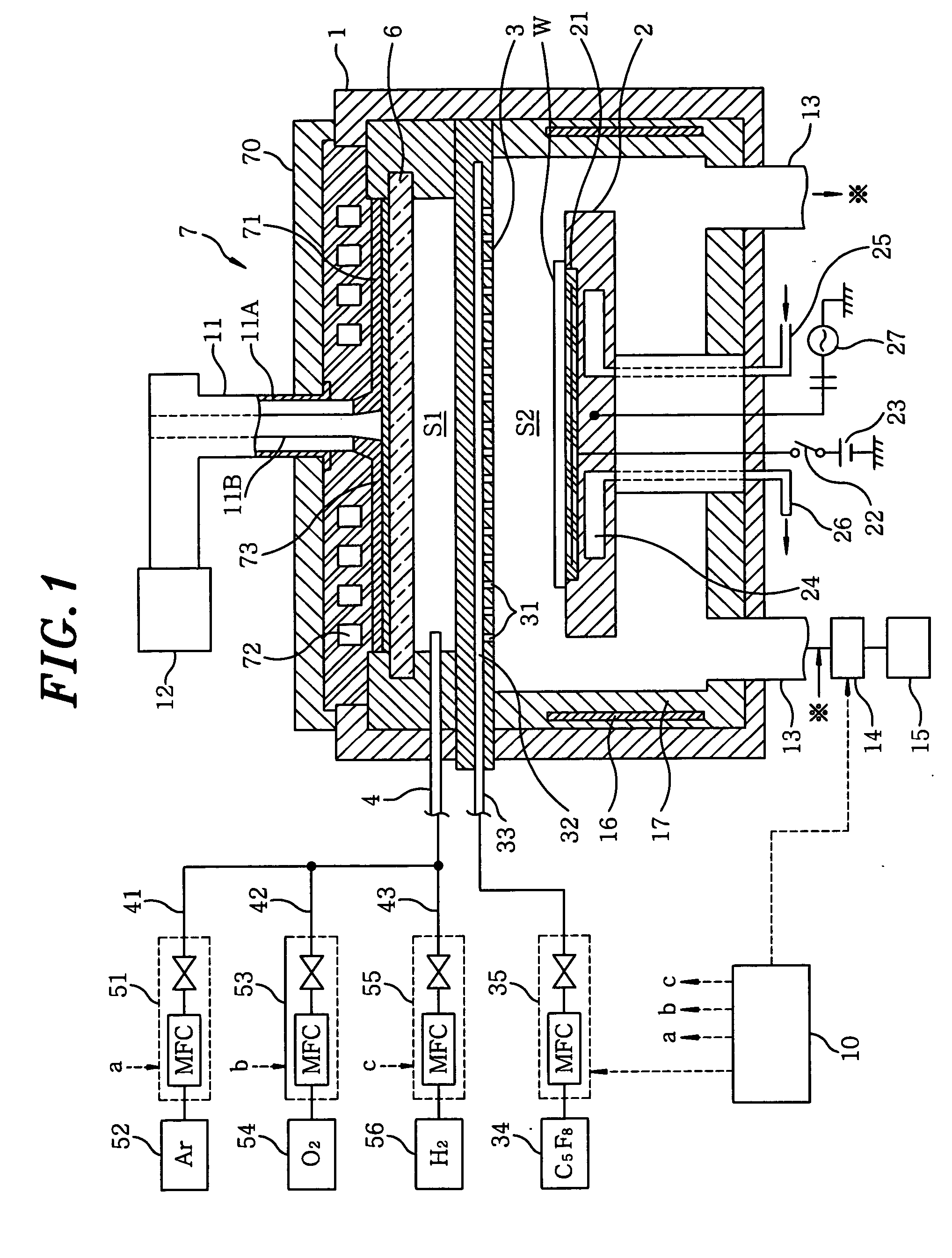
[0043] Hereinafter, a plasma film forming apparatus in accordance with a preferred embodiment of the present invention will be described with reference to FIGS. 1 to 3.

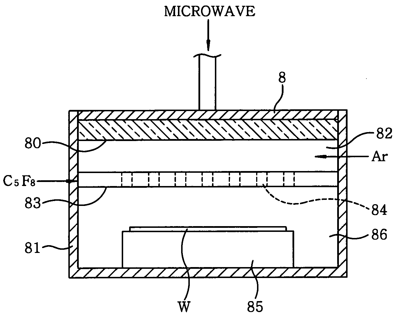
[0044] Reference numeral 1 in FIG. 1 denotes a processing chamber made of, e.g., aluminum. In the processing chamber 1, there are provided a mounting table 2 made of, e.g., aluminum nitride or aluminum oxide for mounting thereon a substrate, i.e., a semiconductor wafer (hereinafter, referred to as “wafer”). The mounting table 2 includes at its top portion an electrostatic chuck 21 whose electrode is connected through a switch 22 to a DC power supply 23. Further, in the mounting table 2, there is provided a temperature control medium channel 24 which serves as a temperature control unit. A coolant introduced through an inlet path 25 flows through the channel 24 to be discharged through an outlet path 26. By using the coolant flowing through the channel 24 and a heater (not shown), the wafer W on the mounting table 2 i...


PUM

PropertyMeasurementUnit
relative dielectric constantaaaaaaaaaa
frequencyaaaaaaaaaa
frequencyaaaaaaaaaa

Abstract

A microwave is radiated into a processing chamber (1) from a planar antenna member of an antenna (7) through a dielectric plate (6). With this, a C5F8 gas supplied into the processing chamber (1) from a gas supply member (3) is changed (activated) into a plasma so as to form a fluorine-containing carbon film of a certain thickness on a semiconductor wafer (W). Each time a film forming process of forming a film on one wafer is carried out, a cleaning process and a pre-coating process are carried out. In the cleaning process, the inside of the processing chamber is cleaned with a plasma of an oxygen gas and a hydrogen gas. In the pre-coating process, the C5F8 gas is changed into a plasma, and a pre-coat film of fluorine-containing carbon thinner than the fluorine-containing carbon film formed in the film forming process is formed.

Description

FIELD OF THE INVENTION [0001] The present invention relates to a method and apparatus for forming a fluorine-containing carbon film, which is used as an interlayer insulating film of a semiconductor device for example, by using a plasma. BACKGROUND OF THE INVENTION [0002] There has been proposed a technology of wiring in a multi-layered structure as an approach for a high integration of a semiconductor device. In order to obtain the multi-layered wiring, an nth layer and an (n+1)th layer are connected to each other through a conductive layer while a thin film called as an interlayer insulating film is formed in areas other than the conductive layer. A SiO2 film is widely used as a typical interlayer insulating film. To further accelerate the speed of an operation of the semiconductor device, it is required to lower the dielectric constant of the interlayer insulating film and to this end, much attention has been paid recently on a fluorine-containing carbon film (fluorocarbon film) ...

Claims


Application Information

Patent Timeline
Patent Type & Authority Applications(United States)
IPC IPC(8): H01L21/26H01L21/42H05H1/24C23C16/26C23C16/44C23C16/511H01J37/32H01L21/31
CPCC23C16/26C23C16/4404C23C16/4405C23C16/511H01J37/32192H01J37/3222H01J37/32238H01J37/3244
Inventor KOBAYASHI, YASUOKAWAMURA, KOHEI
Owner TOKYO ELECTRON LTD
Why Eureka
Try Eureka