Method of timing calibration using slower data rate pattern

a data rate pattern and timing calibration technology, applied in the direction of digital transmission, instruments, generating/distributing signals, etc., can solve the problems of increasing reducing the timing margin for data capture, and correspondingly reducing the timing budget allocated, so as to reduce the overhead of die size and reduce the cost and complexity of system devices. , the effect of simplifying logi

Inactive Publication Date: 2005-09-15
ROUND ROCK RES LLC
View PDF3 Cites 26 Cited by
  • Summary
  • Abstract
  • Description
  • Claims
  • Application Information

AI Technical Summary

Benefits of technology

[0013] The improved technique and apparatus permits the use of any pattern of bits as a calibration test pattern, programmable by the user or using easily-interchangeable hardware. The test bit pattern can thus be adapted to provide a better stimulus for characterizing the timing performance of a particular system or the expected data patterns that the data paths are expected to encounter.
[0014] Because the logic for generating the calibration test pattern is no longer required to be included in each system device (i.e., each logic device no longer requires a shift register for generating a local pseudo-random pattern), the invention simplifies the logic and thus reduces die size overhead for many logic devices. The resulting die size savings desirably reduces the cost and complexity of system devices.

Problems solved by technology

While the timing calibration described above, which is conducted at start-up and reset, has been found to perform adequately in most circumstances, there is a problem in that as the data rate of memory devices is increased, the timing margin for data capture is decreased.
This reduction in uncertainty results in a corresponding decrease in the timing budget allocated to uncertainty and thus an increase in the timing margin for data capture.
Moreover, the calibration bit pattern currently in use, for example the 15-bit pseudo random pattern, may not perform optimally for modern high performance memory systems.
Because current memory devices capture incoming data on both positive and negative going transitions of the clock signal, even when timing calibration is achieved it may not be clear if alignment was achieved on a positive going or negative going clock edge.
Thus, calibration may be achieved in the wrong phase of the clock signal, leading to incorrect sampling of the data during memory access operations, or requiring additional complicated circuitry to ensure that incoming data is synchronized to the proper phase of the clock.

Method used


Image

  • Method of timing calibration using slower data rate pattern
  • Method of timing calibration using slower data rate pattern
  • Method of timing calibration using slower data rate pattern

Examples


Embodiment Construction

[0034] The invention will now be described with respect to the aspect of the invention wherein any pattern of bits may be used as a calibration pattern. In the following, a novel method and associated apparatus is described for transmitting and receiving a calibration bit pattern at a rate slower than a normal operating rate of a receiving logic circuit to ensure correct capture of the calibration bit pattern. However, other methods of ensuring the correct transmission and capture of a calibration pattern at a logic device in a digital circuit are possible, and the invention is not to be limited to any particular method of transmission or capture of digital bits.

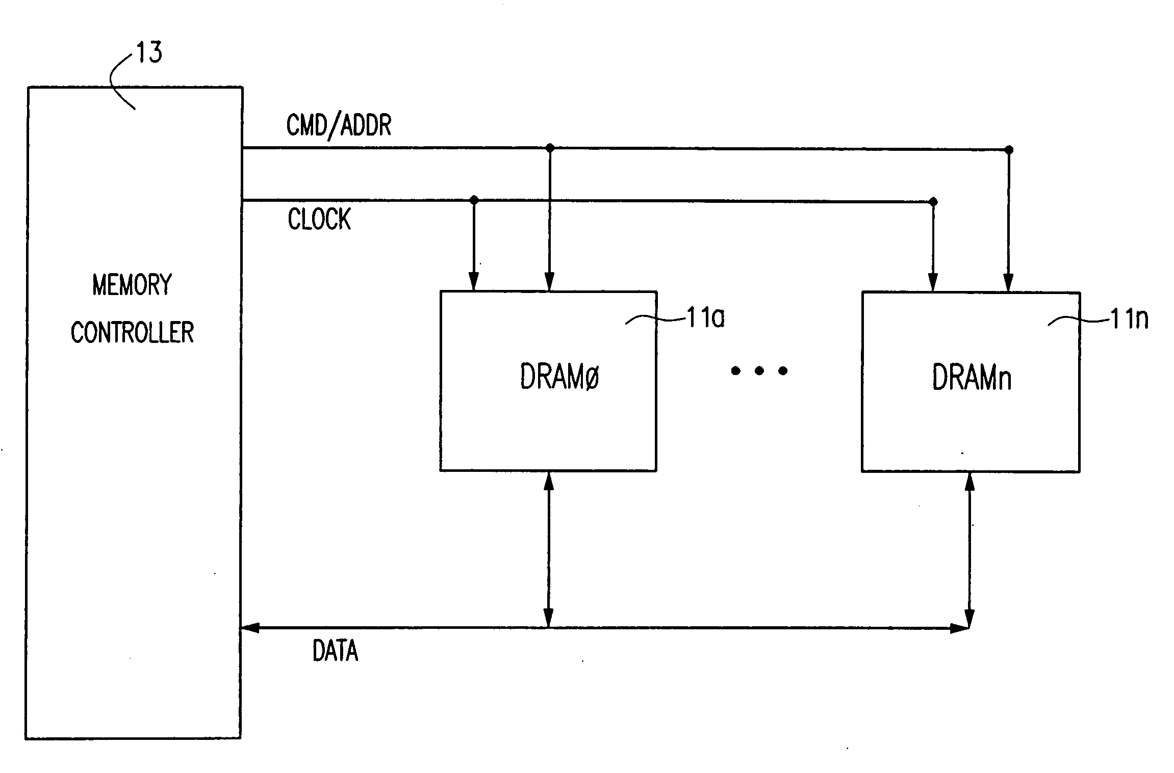
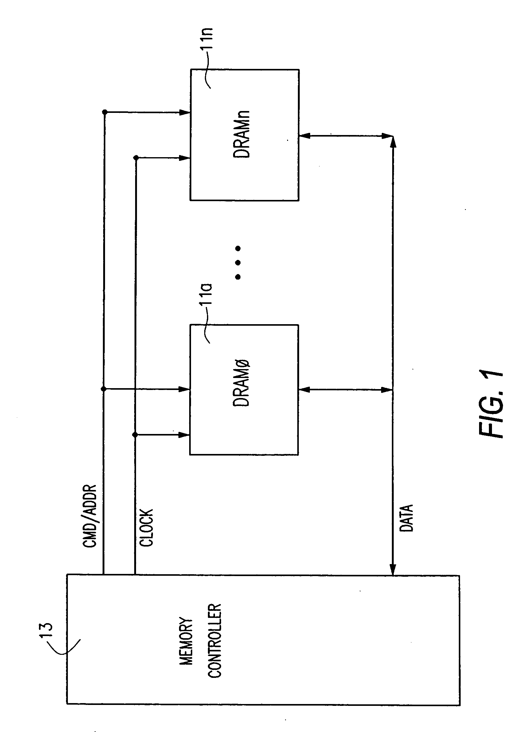
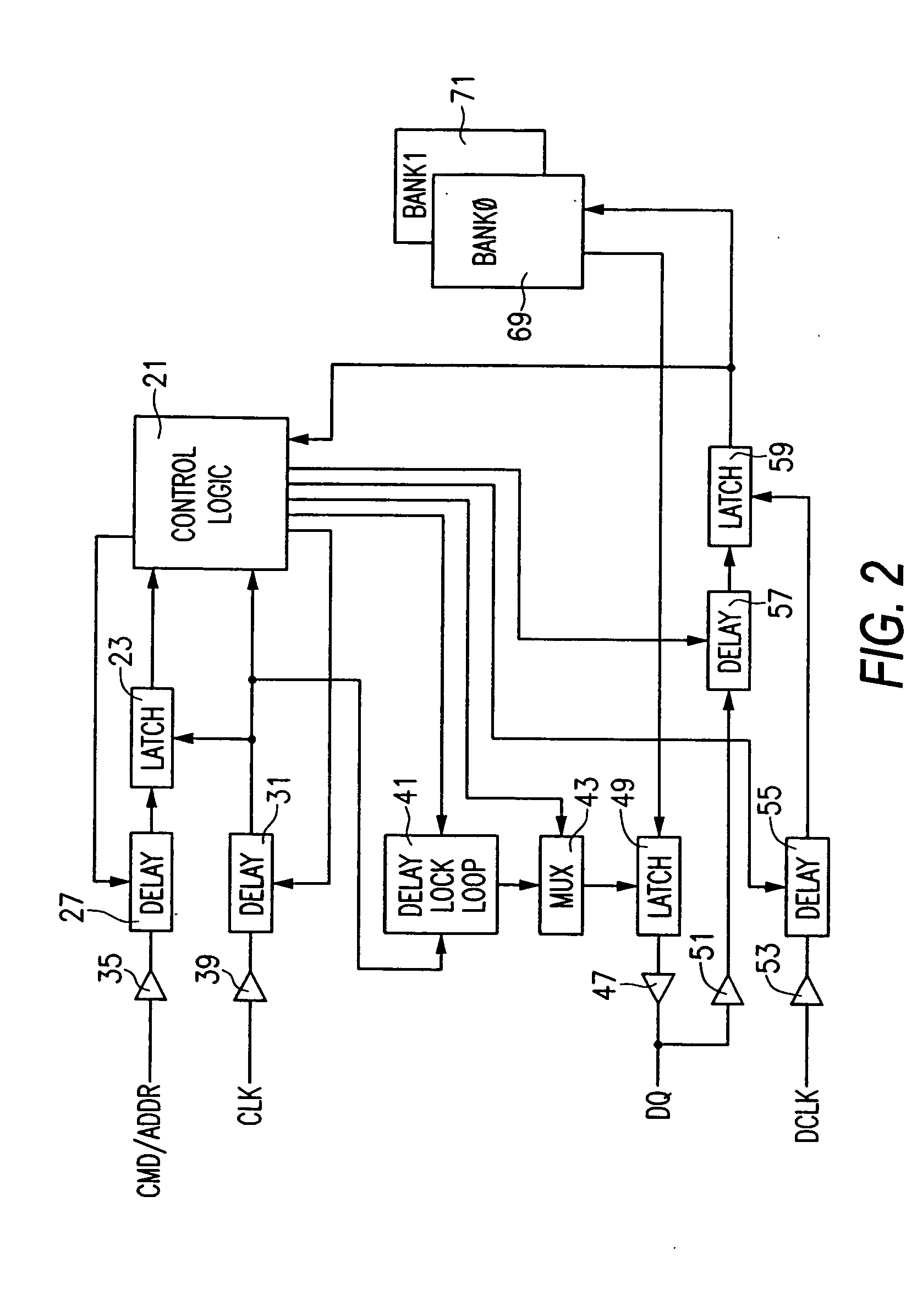
[0035] FIGS. 9(A) and 9(B) show an embodiment of the invention used in an exemplary digital circuit, such as a memory circuit. Referring to FIG. 9(A), a digital circuit topology is shown including two logic devices 101, 103 connected by a bus 107. Each of the logic devices 101, 103 includes a control logic circuit 21, such ...


PUM


Abstract

An improved technique and associated apparatus for timing calibration of a logic device is provided. A calibration test pattern is transferred to a logic device first at a data rate slower than normal operating speed to ensure correct capture of the pattern at the device to be calibrated. Once the pattern is correctly captured and stored, the test pattern is transmitted to the logic device at the normal operating data rate to perform timing calibration. The improved technique and apparatus permits the use of any pattern of bits as a calibration test pattern, programmable by the user or using easily-interchangeable hardware.

Description

FIELD OF THE INVENTION [0001] The present invention relates to calibrating timing of command and data signals on data paths of logic devices, e.g. memory devices, and in particular to using a first data rate slower than the devices' normal operating rate to transfer a calibration bit pattern between logic devices during calibration. BACKGROUND OF THE INVENTION [0002] Memory devices are constantly evolving in the directions of faster speed and higher memory density. To this end, dynamic random access memory (DRAM) devices have evolved from simple DRAM devices to EDO to SDRAM to DDR SDRAM. [0003] One characteristic of modern memory technology is that it may use both the positive- and negative-going edges of a clock cycle to READ and WRITE data to the memory cells and to receive command data from a memory controller. DDR SDRAM represents one example of a modern memory technology that utilizes both positive- and negative-going edges of a clock cycle. [0004] Because of the required high ...

Claims


Application Information

Patent Timeline
Patent Type & Authority Applications(United States)
IPC IPC(8): G01R31/28G01R31/3193G06F1/04G06F11/00G06F13/00G06F13/42G06F19/00G11C29/50H04L5/00
CPCG01R31/31937H03L7/0814G11C7/1078G11C7/1087G11C7/109G11C7/22G11C7/222G11C11/401G11C11/4076G11C11/4093G11C29/02G11C29/023G11C29/028G11C29/50G11C29/50012G11C2207/2254H03L7/0812G11C7/1051
Inventor LEE, TERRY R.RYAN, KEVIN J.JEDDELOH, JOSEPH M.
Owner ROUND ROCK RES LLC
Why Eureka
Try Eureka