Method of making thin-film chip resistor

Inactive Publication Date: 2005-09-22
ROHM CO LTD
View PDF5 Cites 5 Cited by
  • Summary
  • Abstract
  • Description
  • Claims
  • Application Information

AI Technical Summary

Benefits of technology

[0020] According to this method, during the step of forming the resistive element, the masking sheet prevents the resistive element from forming in the lengthwise breaking grooves and the crosswise breaking grooves, or reduces the formation. This shortens the time necessary for the etching that follows, making possible to dramatically reduce a rate of defective products rejected for such reasons as the resistive element o

Problems solved by technology

Moreover, the residue causes another problem in a step which must be done before the cutting.
If the resistive element material B is left in the breaking grooves A1, A2, it becomes impossible to obtain an accurate resistance value, which not only decreases accuracy of the trimming adjustment but also results in poor yield of the product.
Another problem is that even after the material plate A has been cut along the breaking grooves A1, A2, the portions which used to be the breaking grooves A1, A2 still carry the resistive element mat

Method used


Image

  • Method of making thin-film chip resistor
  • Method of making thin-film chip resistor
  • Method of making thin-film chip resistor

Examples


Example

[0062] Hereinafter, modes of embodying the present invention will be described with reference to the drawings.

[0063] Among the drawings, FIG. 10 through FIG. 13 show steps of a method according to a first mode of embodiment.

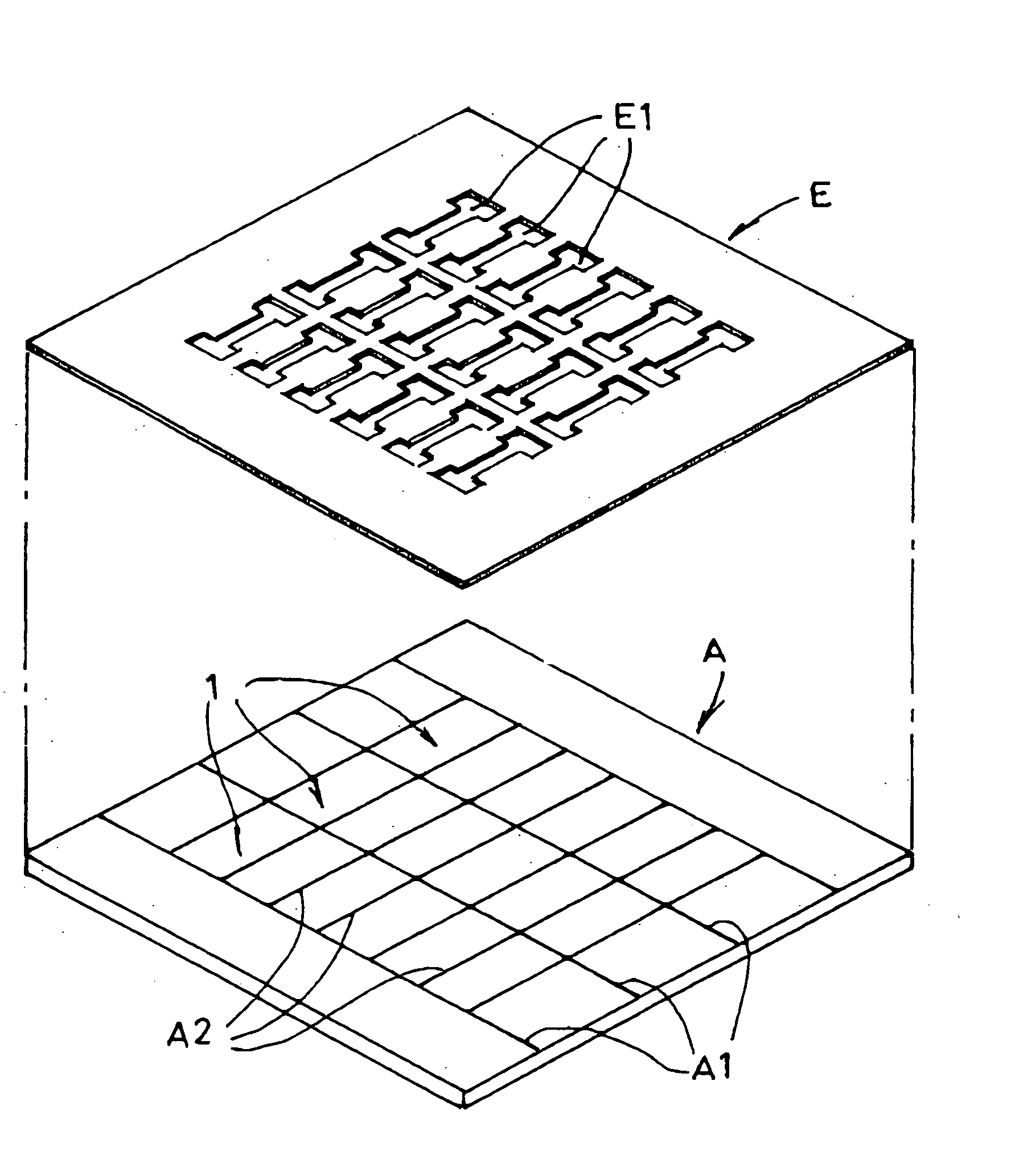
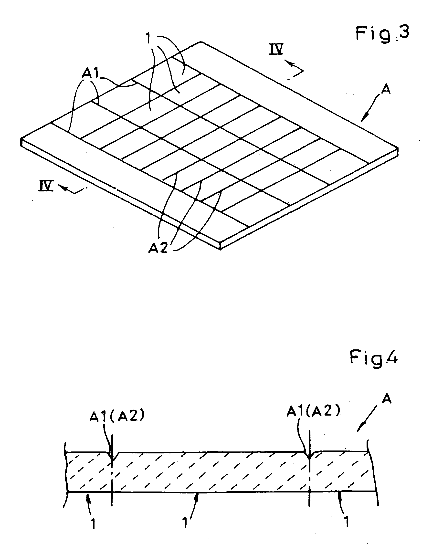
[0064] The method according to the first mode of embodiment includes, as does the conventional method, a step of preparing a material plate A (see FIG. 10) which has a surface provided with lengthwise breaking grooves A1 and crosswise breaking grooves A2 for the purpose of cutting the substrate into a plurality of chip substrates 1. The lengthwise breaking grooves A1 and the crosswise breaking grooves A2 can be formed simultaneously when the material plate A is manufactured. Alternatively, the material plate A may not be formed with the lengthwise breaking grooves A1 and the crosswise breaking grooves A2 at the time of manufacture, and the lengthwise breaking grooves A1 and the crosswise breaking grooves A2 may be formed later using laser beams for example, on ...


PUM

PropertyMeasurementUnit
Widthaaaaaaaaaa
Non-magneticaaaaaaaaaa

Abstract

A method of making a thin-film chip resistor includes: a step of making a material plate A formed with lengthwise breaking grooves A1 and crosswise breaking grooves A2 along which the plate is to be divided into individual chip substrates 1 each to become a chip resistor; and a step of forming a film of resistive element material B by a thin-film process such as spattering, on a surface of the material plate A. The step of thin-film process, in which the resistive element material B is formed, is performed with a masking sheet E placed on the surface of the material plate A, covering only regions including the lengthwise breaking grooves A1 and the crosswise breaking grooves A2.

Description

TECHNICAL FIELD [0001] The present invention relates to a method of making a chip resistor which includes a thin-film resistive element formed by a thin-film process such as spattering and vacuum deposition on a chip substrate provided by a heat resistant insulation material. BACKGROUND ART [0002] A thin-film chip resistor of this kind is disclosed in JP-A 2001-35702 for example, and has a construction as shown in FIG. 1 of the present application. Specifically, the chip resistor includes a chip substrate 1 made of a heat resistant insulation material such as ceramic, which has a surface provided with a thin-film resistive element 2 formed by a thin-film process such as spattering. The resistive element 2 is patterned to have two wide ends 2a, 2b sandwiching a narrow intermediate portion 2c. [0003] The thin-film chip resistor can be of a type shown in FIG. 2-a or a type shown in FIG. 2-b. Specifically, in the type shown in FIG. 2-a, the resistive element 2 has its two wide ends 2a, ...

Claims


Application Information

Patent Timeline
IPC IPC(8): H01C7/00H01C7/02H01C17/00H01C17/075
CPCH01C17/075Y10T29/49085Y10T29/49082H01L27/02
Inventor OSAKI, NOBUOTANIMURA, MASANORI
Owner ROHM CO LTD
Why Eureka
Try Eureka