Scanning electron microscope and a method for evaluating accuracy of repeated measurement using the same

a scanning electron microscope and repeated measurement technology, applied in the field of scanning electron microscopes, can solve the problems that the influence of fluctuations in micro-minute shape cannot be ignored in measurement errors, and achieve the effect of eliminating the influence of contamination, high degree of accuracy, and eliminating measurement errors

Inactive Publication Date: 2005-09-22
HITACHI HIGH-TECH CORP
View PDF3 Cites 29 Cited by
  • Summary
  • Abstract
  • Description
  • Claims
  • Application Information

AI Technical Summary

Benefits of technology

[0016] According to the present invention, it is possible to eliminate a measurement error caused by the change in micro-minute shape such as the line edge roughness included in a wiring pattern, and to present the measurement repeatability as a tool with a high degree of accuracy of about 1 to 2 nm or less without being influenced by a target to be measured.
[0017] Furthermore, according to the present invention, it is possible to effectively eliminates the influence of the contamination appearing when measuring the same sample a plurality of times, and to evaluate the measurement repeatability as the tool with a high degree of accuracy of about 1 to 2 nm or less.

Problems solved by technology

Accordingly, it is expected that in future a measurement error caused by the influence of fluctuations in micro-minute shape cannot be ignored in association with a dimension error which a CDSEM might generate.

Method used


Image

  • Scanning electron microscope and a method for evaluating accuracy of repeated measurement using the same
  • Scanning electron microscope and a method for evaluating accuracy of repeated measurement using the same
  • Scanning electron microscope and a method for evaluating accuracy of repeated measurement using the same

Examples


first embodiment

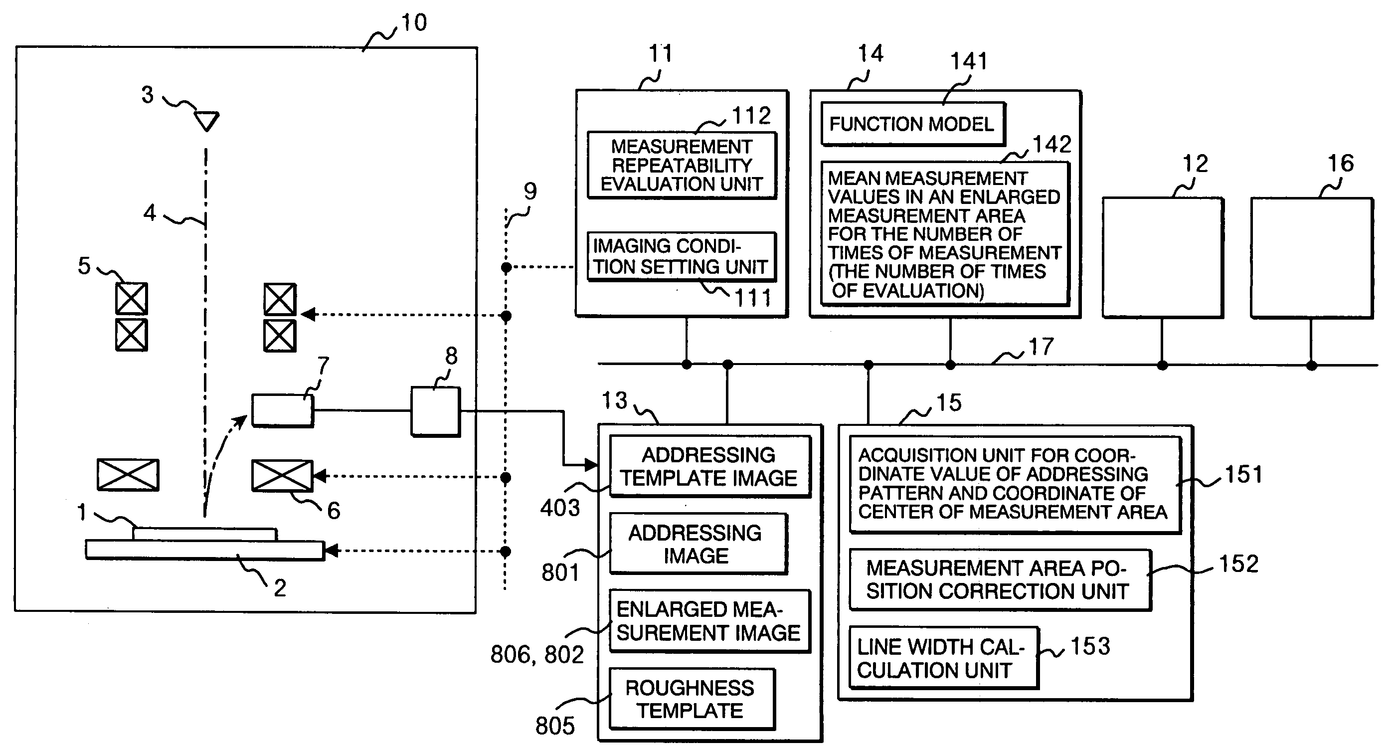
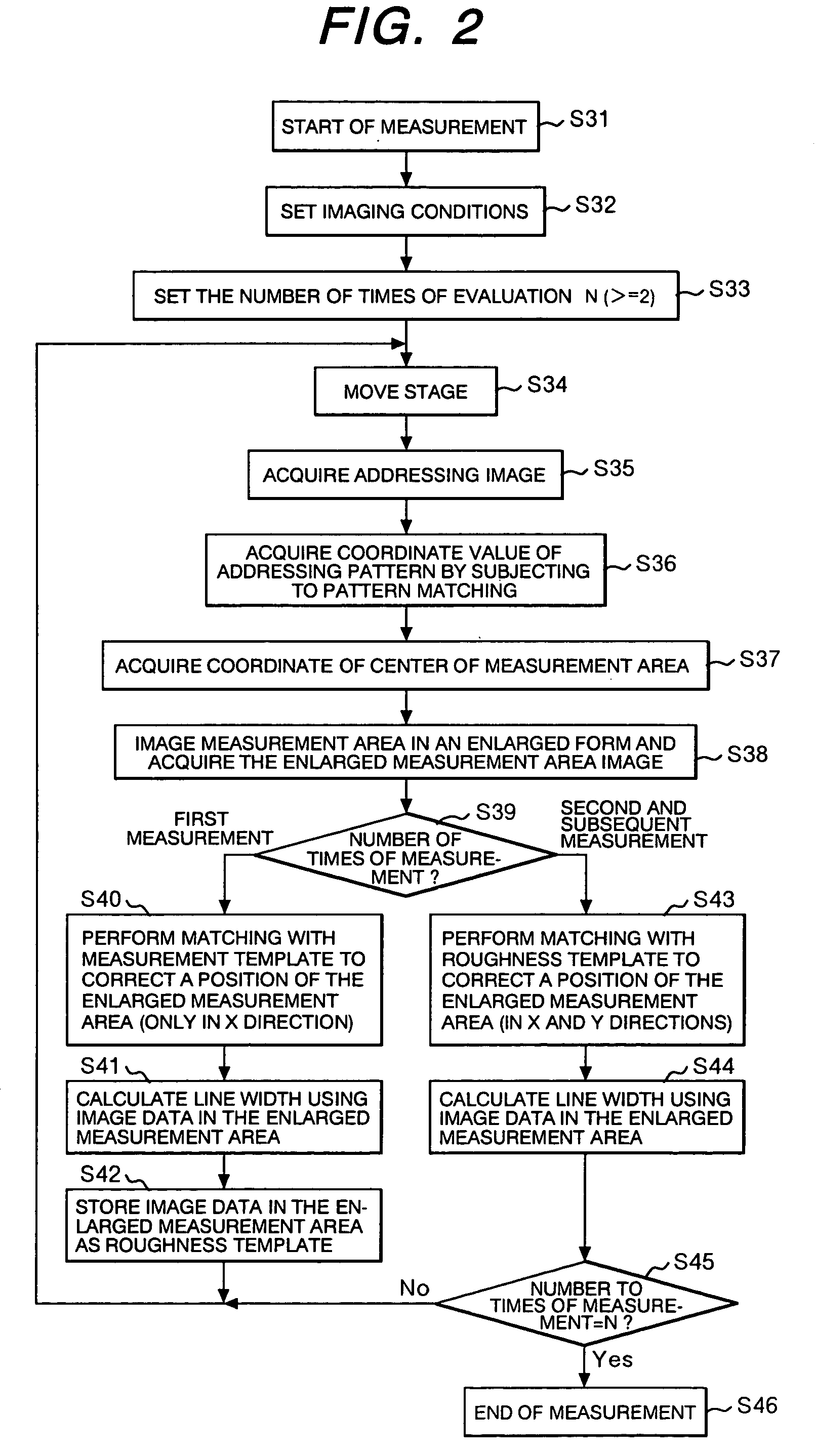
[0039] Next, a sequence of measuring a plurality of times the line width (CD) of a pattern in the same measured part (typical dimensions or shape of the pattern (measurement values at a plurality of points)) using a CDSEM according to the present invention will be described with reference to FIG. 2 or 5.

[0040] In the first place, the total control unit 11 starts measurement (S31). Next, the imaging condition setting unit 111 of the total control unit 11 sets imaging conditions of the electro-optical system 10 in the CDSEM (an acceleration voltage of an electron beam, a beam current, the imaging magnification, the amount of dose, and the like) (S32). Then, a user uses an input means 12 to specify the number of times of measurement (the number of times of evaluation) N for the total control unit 11 (S33). Main imaging conditions which should be set for the imaging of an image by a SEM include: an acceleration voltage of an incident beam; a beam current; the imaging magnification; and ...

second embodiment

[0059]FIG. 6 illustrates a process flow of the To begin with, the imaging condition setting unit 111 of the total control unit 11 sets imaging conditions (an acceleration voltage of an electron beam, a beam current, the imaging magnification, the amount of dose, and the like) for the CDSEM (S32). Next, an enlarged measurement image at a measurement point is acquired. After that, the roughness template 805 is extracted from the enlarged measurement image, and is then stored in the storage unit 13 (S50). In this processing, the acquisition of the enlarged image by moving the stage 2, the extraction of the roughness template 805 from the acquired enlarged image, and storing of the roughness template 805, may also be performed by manual operation, or may also be automatically performed using the imaging sequence shown in FIG. 2. Next, N, which is the number of times of measurement, is specified for the total control unit 11 by a user (S33). Then, under the imaging conditions set for th...


PUM

PropertyMeasurementUnit
roughnessaaaaaaaaaa
sizeaaaaaaaaaa
scanning electron microscopeaaaaaaaaaa

Abstract

The present invention relates to a CDSEM (scanning electron microscope) capable of evaluating and presenting the measurement repeatability as a tool with a high degree of accuracy without being influenced by fluctuations in micro-minute shape that tend to increase with the microminiaturization of semiconductor patterns, and to a method for evaluating accuracy of repeated measurement using the scanning electron microscope. There is provided a function whereby when measuring a plurality of times the same part to be measured, by making use of a micro-minute pattern shape such as the roughness included in the pattern, pattern matching with a roughness template image is performed to correct two-dimensional deviation in position of the part to be measured on an enlarged measurement image acquired, and then an enlarged measurement area image is extracted and acquired. This makes it possible to eliminate variation in measurements caused by the micro-minute pattern shape.

Description

BACKGROUND OF THE INVENTION [0001] The present invention relates to an electron microscope for performing CD measurement of semiconductor patterns having various kinds of shapes and dimensions, and more particularly to a scanning electron microscope having a function suitable for managing the measurement precision, and to a method for evaluating accuracy of repeated measurement using the scanning electron microscope. [0002] In a semiconductor wafer manufacturing process, the microminiaturization of thin film patterns which are formed on a wafer in a multilayer structure rapidly progresses. Accordingly, the importance of process monitoring which monitors whether or not those patterns are formed on the wafer according to the design is more and more increasing. Above all, as far as transistor gate wiring and metal wiring made of aluminum, copper, or the like formed on a wafer, are concerned, there is a close relationship between the line width and device operation characteristics, and ...

Claims


Application Information

Patent Timeline
Patent Type & Authority Applications(United States)
IPC IPC(8): G01N23/00G01N23/225G01B15/00G03C5/00H01J37/28
CPCG01N23/225
Inventor NAKAGAKI, RYOKAWADA, HIROKISHISHIDO, CHIEOOSAKI, MAYUKA
Owner HITACHI HIGH-TECH CORP
Why Eureka
Try Eureka