

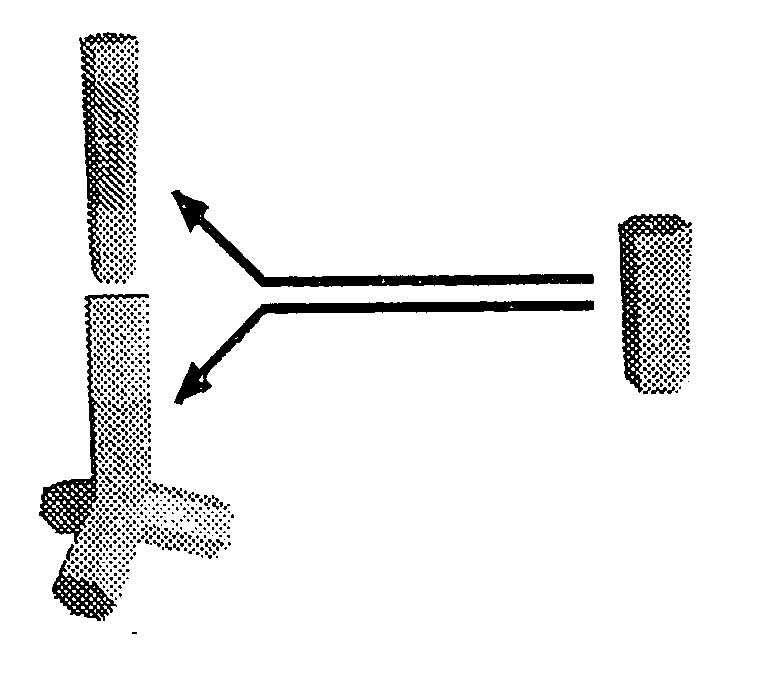
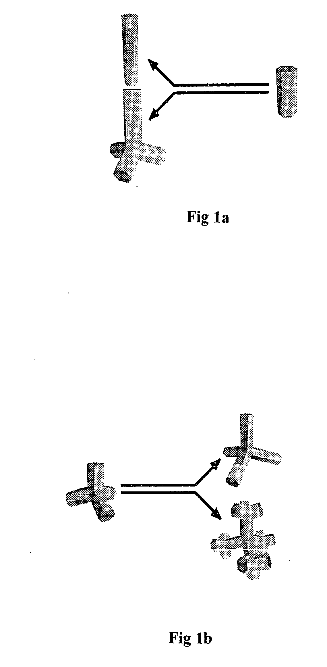
Nanocrystals with linear and branched topology
a technology of nanocrystals and branched topology, which is applied in the field of colloidal semiconductor nanocrystals, can solve the problems of increasing the occurrence of surface trap-states, limiting the growth of heterostructures in colloidal nanocrystals, and limiting the control of the electronic structure of concentric heterostructures, etc., to achieve the effect of simple geometry and simple structur
- Summary
- Abstract
- Description
- Claims
- Application Information
AI Technical Summary
Problems solved by technology
Method used
Image

Examples
examples
[0058] The examples provided herein are provided as examples and not limitations, wherein a number of modifications of the exemplified process are contemplated and within the scope of the present invention.
[0059] Materials. Dimethylcadmium (Cd(CH3)2, 97%), tri-n-octylphosphine (C24H51P or TOP) and tri-n-butylphosphine (C12H27P or TBP, 99%) were purchased from Strem. Cd(CH3)2 was vacuum transferred and stored at −35° C. under argon. Selenium (Se) (99.999%), tri-n-octylphosphine oxide (C24H51OP or TOPO, 99%), diethylzinc (C4H10Zn, or Et2Zn, 1.0 M solution in heptane), cadmium oxide (CdO) and hexamethyldisilathiane (C6H18Si2S or (TMS)2S) were purchased from Aldrich. Hexylphosphonic acid (C6H15O3P or HPA 99%) was purchased from Organometallics Inc., tetradecylphosphonic acid (C14H31O3P or TDPA, 98%) was purchased from Alfa, and octadecylphosphonic acid (C18H39O3P or ODPA) was purchased from PolyCarbon Industries. All solvents used were anhydrous, purchased from Aldrich and used without...
example i
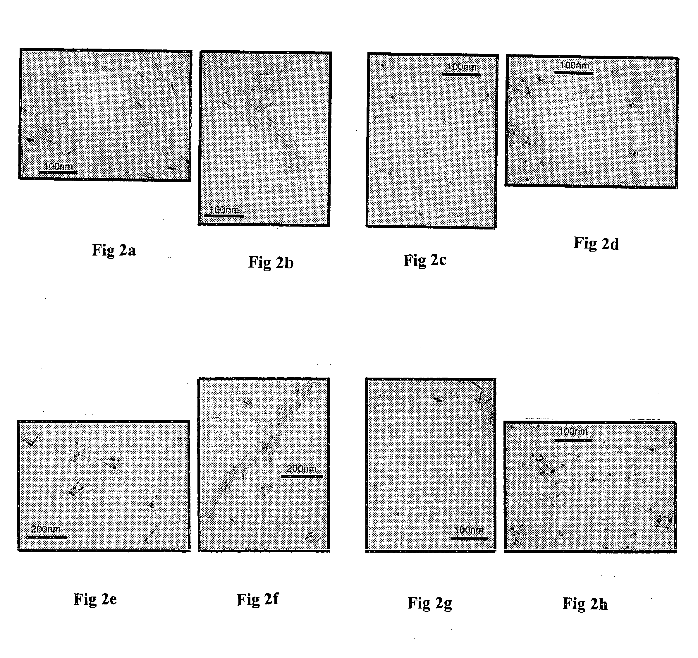
[0060] Synthesis of CdSe Rods. All manipulations were performed using standard air-free techniques, unless otherwise stated. In a typical synthesis, a mixture of HPA, TDPA and TOPO was degassed at 120° C. for 1 hour in a 50 ml 3-neck flask connected to a Liebig condenser, after which 0.5 g of the Cd precursor solution was added drop wise. The resulting mixture was then heated to 360° C. and 2.5 g of the Se precursor solution was quickly injected. After injection, the temperature dropped to 290° C. and was maintained at this level throughout the synthesis. When desired, the synthesis was stopped by removing the heating mantle and by rapidly cooling the flask
[0061] After cooling the solution to 50° C., 4.0 ml of methanol was added to precipitate the rods from the solution. This suspension was then transferred to a dry box, where it was centrifuged and the precipitate was washed three times with methanol. The final precipitate was then dried under Ar and stored in the dry box. Due to ...
example ii
[0062] CdSe nanorods were prepared by dissolving 104 mg of CdO in 0.81 g of octadecylphosphonic acid and 3.19 g of tri(n-octyl)phosphine oxide at 300° C. At 280° C., 15.8 mg of selenium dissolved in 320 mg of tri(n-octyl)phosphine (TOP) were injected and the CdSe nanorods grew for four minutes. At 290° C., 34 mg of tellurium dissolved in 306 mg of TOP were injected and CdTe branches grew for six minutes before the heat was removed to stop the reaction.
PUM
| Property | Measurement | Unit |
|---|---|---|
| angle | aaaaa | aaaaa |
| angle | aaaaa | aaaaa |
| angle | aaaaa | aaaaa |
Abstract
Description
Claims
Application Information