Memory cell having an electric field programmable storage element, and method of operating same

a memory cell and electric field technology, applied in the field of memory cells, arrays and/or devices, can solve the problems of heat dissipation, timing, power consumption, complex architecture, etc., and achieve the effects of reducing the cost of manufacturing, and improving the efficiency of the storage devi

Inactive Publication Date: 2005-09-29
GREER EDWARD C +2
View PDF65 Cites 21 Cited by
  • Summary
  • Abstract
  • Description
  • Claims
  • Application Information

AI Technical Summary

Benefits of technology

[0026] The memory cell of this aspect also includes a second electric field programmable bi-stable element which is connected to the second semiconductor transistor. The second electric field programmable bi-stable element includes first and second electrodes and at least one electric field programmable film disposed between the first and second electrodes. The electric field programmable film of the second electric field programmable element includes at least two resistance states, including a first resistance state and a second resistance state.

Problems solved by technology

Although devices including such memory cells have been technically and commercially successful, they have a number of shortcomings, including, for example, complex architectures, density constraints, and relatively high fabrication costs.
This may raise issues pertaining to heat dissipation, timing, and power consumption.
In addition, although certain integration densities can be achieved, such devices tend to be limited or restricted with respect to the size of the memory cell.
As such, conventional DRAMs employing one transistor—one capacitor memory cells, tend to be limited or restricted with respect to the size of the memory cell as well as layout to a single plane.
Non-volatile semiconductor devices avoid certain issues prevalent in volatile semiconductor devices but often suffer from reduced data storage capability, capacity and / or density as a result of higher complexity in cell and circuit design.
The higher complexity often results in higher production costs.
However, many currently known bistable films are inhomogeneous, multilayered composite structures fabricated by evaporative methods, which are expensive and often difficult to control.
In addition, these bistable films do not afford the opportunity for fabricating films in topographies ranging from conformal to planar.
Bistable films fabricated using polymer matrices and particulate matter are generally inhomogeneous and therefore unsuitable for fabricating submicrometer and nanometer-scale electronic memory and switching devices.
Still other bistable films can be controllably manufactured by standard industrial methods, but their operation requires high temperature melting and annealing at grid intersection points.
Such films generally suffer from thermal management problems, have high power consumption requirements, and afford only a small degree of differentiation between the “conductive” and “nonconductive” states.
Furthermore, because such films operate at high temperatures, it is difficult to design stacked device structures that allow high density memory storage.

Method used


Image

  • Memory cell having an electric field programmable storage element, and method of operating same
  • Memory cell having an electric field programmable storage element, and method of operating same
  • Memory cell having an electric field programmable storage element, and method of operating same

Examples


Embodiment Construction

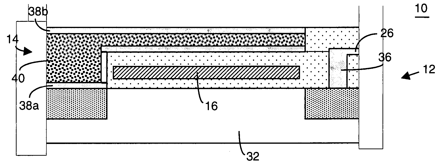
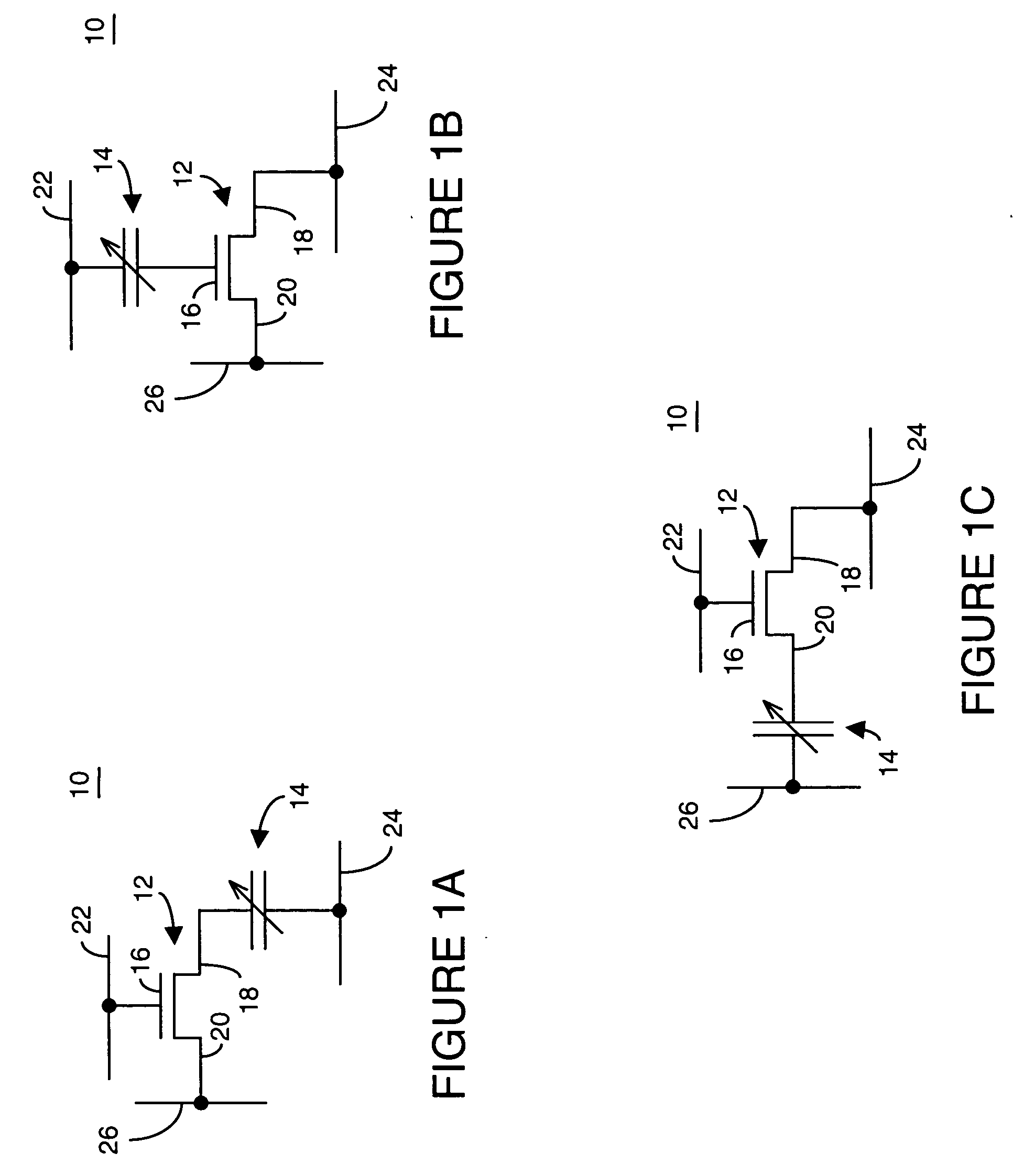
[0072] In a first aspect, disclosed is a memory cell having an access transistor and an electric field programmable bi-stable element. The access transistor may be a (N-channel or P-channel) MOSFET transistor having a gate, source or drain region coupled to the electric field programmable bi-stable or multi-stable element (hereinafter collectively, “electric field programmable bi-stable element”, unless expressly indicated otherwise). The access transistor facilitates selective and controllable programming and reading of the electric field programmable bi-stable element.

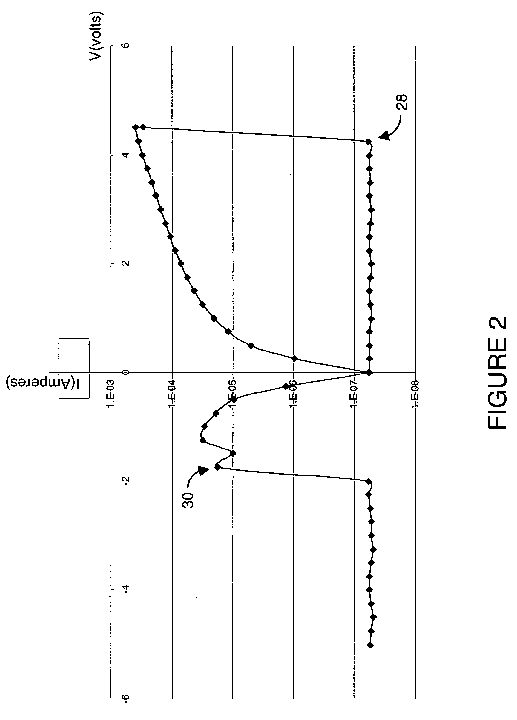
[0073] In one embodiment, the electric field programmable bi-stable element provides two or more different resistance characteristics; each resistance characteristic is representative of one data state (for example, an analog or digital state). The electric field programmable bi-stable element may be comprised of one or more electric field programmable films including an electron donor and / or an electron acceptor an...


PUM


Abstract

Disclosed is a memory cell having an access transistor and an electric field programmable bi-stable element. The access transistor may be a (N-channel or P-channel) MOSFET transistor having a gate, source or drain region coupled to the electric field programmable bi-stable or multi-stable element (hereinafter collectively, “bi-stable element” unless expressly indicated otherwise). The access transistor facilitates selective and controllable programming and reading of the electric field programmable bi-stable element. Also disclosed is a plurality of memory cells, each having a unique, different and/or distinct electric field programmable bi-stable element and a common access transistor and a common access transistor. In yet another aspect, a differential memory cell having a plurality of memory cells configured to store complementary data states is disclosed. The differential memory cell includes first memory cell and second memory cell wherein the first memory cell maintains a complementary state relative to second memory cell. The first and second memory cells include a common access transistor and unique, different and/or distinct electric field programmable bi-stable element, or each includes an access transistor and an electric field programmable bi-stable element. Finally, a complementary memory cell having an N-channel type memory cell (an N-channel access transistor and an electric field programmable bi-stable element) and a P-channel type memory cell (a P-channel access transistor and an electric field programmable bi-stable element) is disclosed.

Description

CROSS-REFERENCE TO RELATED APPLICATIONS [0001] This application claims priority to U.S. Provisional Application Ser. No. 60 / 556,246, entitled “Memory Devices based on Electric Field Programmable Films”, filed Mar. 24, 2004; the contents of which are incorporated by reference herein in their entirety.BACKGROUND [0002] This invention relates to a memory cell, array and / or device and method of controlling and / or operating the memory cell, array and / or device; and more particularly, in one aspect, to a memory cell, and array and / or device including a plurality of such memory cells, wherein the memory cells each include an electric field programmable film to store an electrical charge which is representative of a data state. [0003] There are many different types and / or forms of memory cells, arrays and devices. Such devices may be classified generally into two different types, namely volatile (for example, dynamic random access memory (“DRAM”) and static random access memory (“SRAM”)), a...

Claims


Application Information

Patent Timeline
Patent Type & Authority Applications(United States)
IPC IPC(8): G11C11/56G11C11/22G11C13/00G11C13/02H01L27/10H01L27/105H01L45/00
CPCB82Y10/00G11C11/22G11C11/5664G11C11/5685G11C13/0007G11C13/0009G11C2213/79G11C13/003G11C2213/15G11C2213/31G11C2213/71G11C2213/78G11C13/0014H01L27/10
Inventor GREER, EDWARD C.MURPHY, ROBERT J.SZMANDA, CHARLES R.
Owner GREER EDWARD C
Why Eureka
Try Eureka