Shift register that suppresses operation failure due to transistor threshold variations, and liquid crystal driving circuit including the shift register

a transistor threshold variation and shift register technology, applied in the direction of television systems, counting chain synchronous pulse counters, instruments, etc., can solve the problems of unfavorable repetitive voltage application, complex circuit structure, unstable circuit operation, etc., to reduce the voltage application time, easy to flow, and small area

Inactive Publication Date: 2005-09-29
ONANOVICH GROUP
View PDF1 Cites 67 Cited by
  • Summary
  • Abstract
  • Description
  • Claims
  • Application Information

AI Technical Summary

Benefits of technology

[0042] In the shift register according to the present invention, therefore, the second transistor and the third transistor are turned on when the clock terminal is switched low (i.e., when the voltage from the output terminal of the input diode in the following stage turns on the first transistor in the following stage), and both terminals of the capacitor are connected to the clock terminal. Thus, both terminals of the capacitor are discharged by the clock terminal to reset the application of a voltage to the control electrode of the first transistor, thereby reducing the voltage application time.
[0043] In the shift register according to the present invention, the input diode may be a transistor having a small area for a required current capacity. Thus, a compact diode that allows a predetermined current to easily flow can be formed.
[0044] The shift register may be configured such that a first shift register is divided into a plurality of blocks and is activated block-by-block by a second shift register. Thus, the first shift register that shifts the output signals can be selectively activated so as not to place stress on the transistor more than necessary to prevent characteristic changes while reducing the consumption power.
[0045] In another aspect of the present inven

Problems solved by technology

Due to the circuit design with limited flexibility, for example, characteristic deterioration of the output transistor 52 can cause unstable circuit operation.
This can cause problems of a complex circuit structure for applying a clock signal to a control electrode of an intermediate transistor and excessive stress placed on other transistors.
In particular, it is undesirable to apply repetitive voltages, e.g., clock signals, to the control electrode, as below.
As is well known in the

Method used


Image

  • Shift register that suppresses operation failure due to transistor threshold variations, and liquid crystal driving circuit including the shift register
  • Shift register that suppresses operation failure due to transistor threshold variations, and liquid crystal driving circuit including the shift register
  • Shift register that suppresses operation failure due to transistor threshold variations, and liquid crystal driving circuit including the shift register

Examples


first embodiment

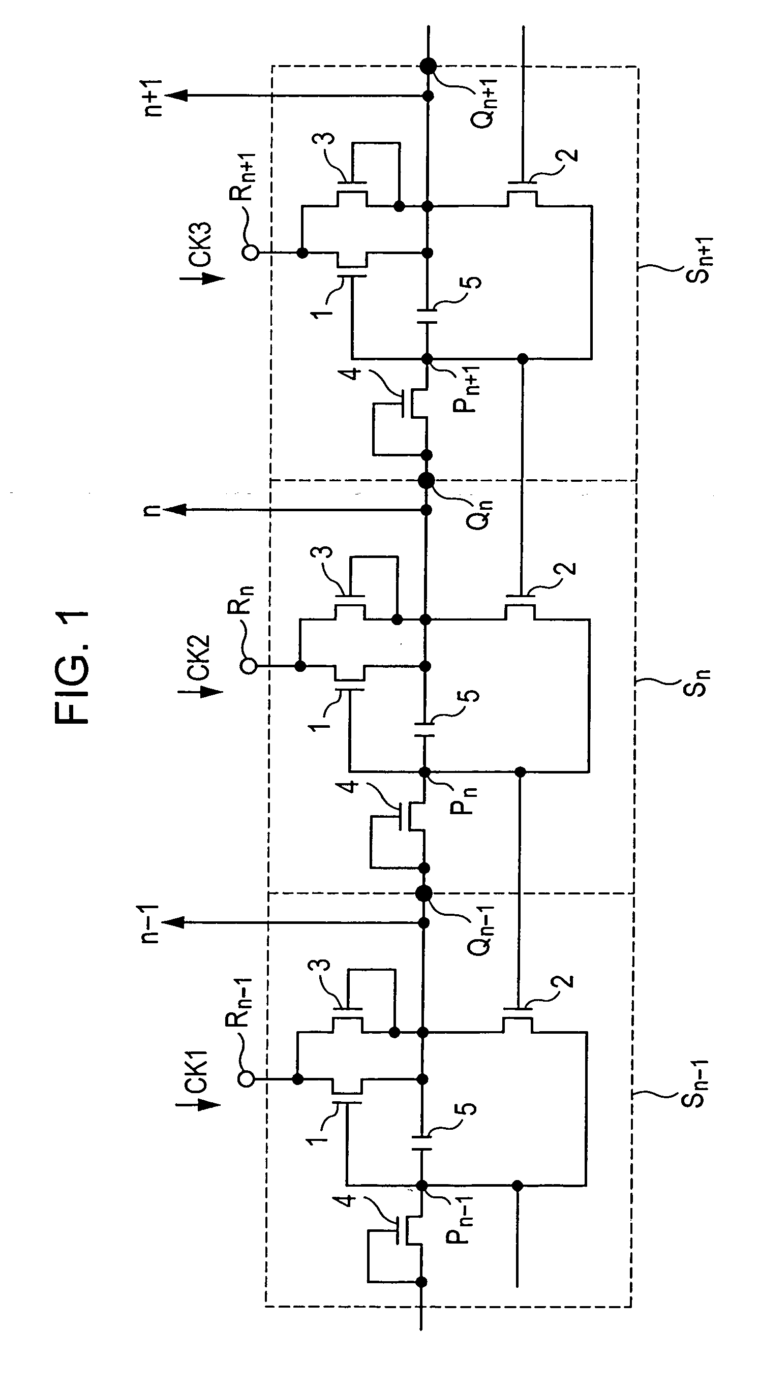
[0059]FIG. 1 is a circuit diagram of a shift register according to a first embodiment of the present invention, showing three stages n−1, n, and n+1 of the shift register, by way of example.

[0060] These stages have a similar structure, and will be described in the context of the stage n. The stage n includes transistors 1, 2, 3, and 4 and a capacitor 5. The transistors 1, 2, 3, and 4 may be n-channel metal insulator semiconductor (MIS) transistors.

[0061] The transistor 4 is a diode-connected transistor between an input terminal Qn−1 (or an output terminal of an (n−1)-th stage Sn−1) and a first terminal of the capacitor 5 (or a node Pn). The diode formed of the transistor 4 is forward connected to the capacitor 5 from the input terminal Qn−1.

[0062] A source terminal of the transistor 4 is a connected to the first terminal of the capacitor 5, and a drain terminal and a control electrode of the transistor 4 are connected to the input terminal Qn−1.

[0063] The transistor 1 has a drai...

second embodiment

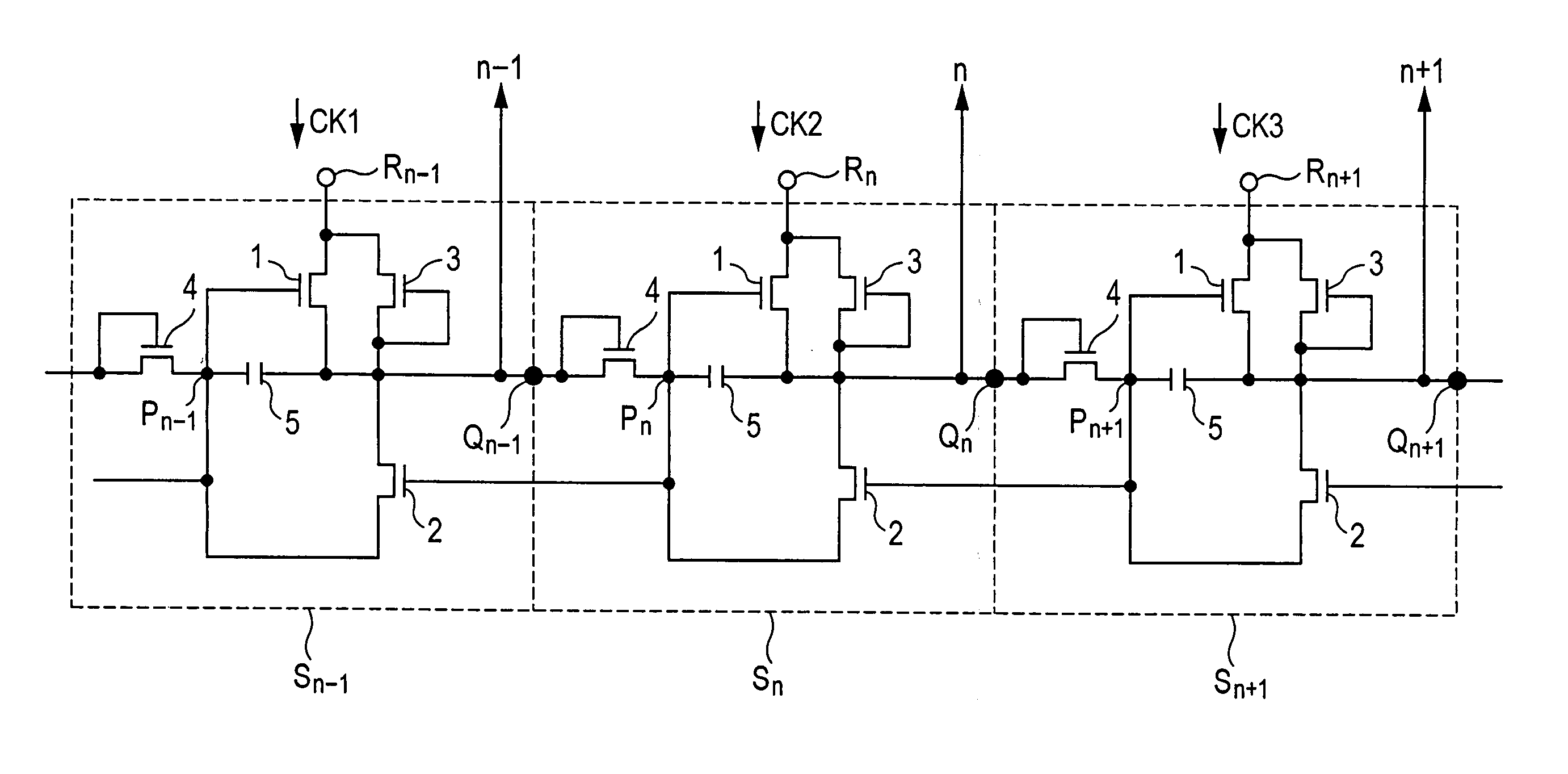
[0094]FIG. 3 is a circuit diagram of a shift register according to a second embodiment of the present invention, showing three stages n−1, n, and n+1 of the shift register, by way of example.

[0095] The shift register according to the second embodiment is different from that according to the first embodiment in that the control electrode of the pull-down transistor 3 and the control electrode of the clamping transistor 2 in the stage Sn are connected to the output node of the transistor 4 in the following stage Sn+1. Similar components to those shown in FIG. 1 are assigned the same reference numerals, and a description thereof is omitted.

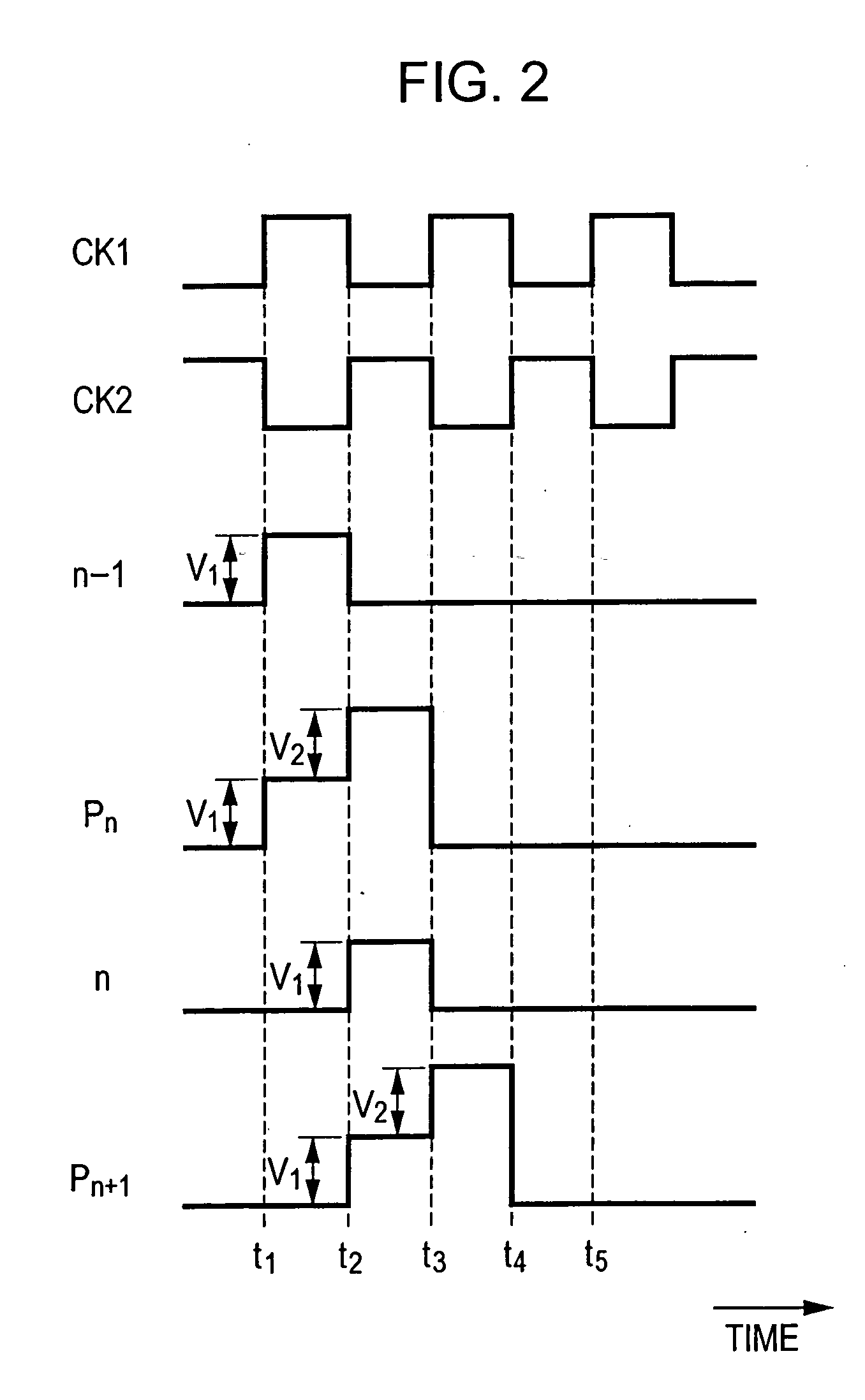
[0096] The shift register according to the second embodiment performs a similar operation to that of the shift register according to the first embodiment described with reference to the timing chart shown in FIG. 2, except that it is responsive to three-phase clock signals. FIG. 4 is a timing chart showing the operation of the shift register accord...

third embodiment

[0100]FIG. 5 is a circuit diagram of a shift register according to a third embodiment of the present invention, showing three stages n−1, n, and n+1, of the shift register, by way of example.

[0101] The shift register according to the third embodiment is different from that according to the second embodiment in that the clamping transistor 2 and the pull-down transistor 3 are connected in parallel with respect to the clock terminal and the transistors 2 and 3 discharge the charge accumulated in the connection node and the output terminal to the clock terminal, respectively.

[0102] That is, when the clocks CK1, CK2, and CK3 are phase-shifted, the charge accumulated in the capacitor 5 in a given stage is discharged. When the capacitor 5 in the following stage is charged, a high-level output signal is output.

[0103] The shift register according to the third embodiment performs a similar operation to that according to the second embodiment described with reference to the timing chart sh...


PUM


Abstract

A shift register having a plurality of stages connected in cascade shifts an output signal by a plurality of clocks having different phases. Each of the stage includes an input diode to which a signal is input from a preceding stage, a capacitor for holding charge having a voltage level of the input signal, a first transistor that is turned on or off by the held voltage level to output an output signal to a following stage in synchronization with a clock signal, and a second transistor connected between the input diode and an output terminal. A control electrode of the second transistor is connected to the input diode in the following stage. The second transistor has a clamping function for discharging the accumulated charge and turning off the first transistor when the clock signal is phase-shifted.

Description

BACKGROUND OF THE INVENTION [0001] 1. Field of the Invention [0002] The present invention relates to a shift register and to a liquid crystal driving circuit including the same. More specifically, the present invention relates to a shift register used in a liquid crystal display for supplying scanning drive signals, and to a liquid crystal driving circuit including the shift register. [0003] 2. Description of the Related Art [0004] Active-matrix liquid crystal displays (LCDs) used in, for example, computers and televisions include an array of video signal lines (source lines) and scanning drive signal lines (gate lines), and switching devices, such as thin-film transistors (TFTs), disposed at intersections of the video signal lines and the scanning drive signal lines for driving liquid crystal of pixels. [0005] Scanning drive signals are supplied to the scanning drive signal lines to sequentially scan the signal lines so that all switching devices on a given scanning drive signal li...

Claims


Application Information

Patent Timeline
IPC IPC(8): G09G3/20G02F1/133G09G3/36G11C19/00G11C19/18H04N5/66
CPCG11C19/184G09G3/3677G09G3/36G11C19/28H03K23/44G09G3/20
Inventor IWASAKI, CHISATOFUJIYOSHI, TATSUMIYAMADA, YUKIMITSUKIKUCHI, KOJI
Owner ONANOVICH GROUP
Why Eureka
Try Eureka