Feed-through process and amplifier with feed-through

a technology of feed-through and amplifier, which is applied in the direction of basic electric elements, semiconductor/solid-state device manufacturing, electrical equipment, etc., can solve the problems of limiting the possibility of obtaining a batch process and a great risk of shattering the wafer

Inactive Publication Date: 2005-09-29
OTICON
View PDF4 Cites 19 Cited by
  • Summary
  • Abstract
  • Description
  • Claims
  • Application Information

AI Technical Summary

Benefits of technology

[0018] The membrane-like structure is composed of local parts of the front side electric insulation and KOH etch-resistant metallic layer(s). In an embodiment of the invention the membrane like structure is etched from the back side through the formed holes in the semiconductor wafer. Opening of the through-holes in this way is advantageous, as the semiconductor wafer itself works as the etch mask, and a front side photolithographic process is avoided.

Problems solved by technology

In some cases it is a problem to provide sufficient space also for the bondpads for in / out signals and for power supply for the IC on the surface when also the electric components are placed here.
This has proved to be cumbersome, and there is a great risk of shattering the wafer due to mechanical stressing of the fragile wafer caused by the bulky mechanical fixture or due to pressure differences between front and back side of the wafer occurring during processing.
In addition the use of a mechanical fixture hampers the possibility of obtaining a batch process.

Method used


Image

  • Feed-through process and amplifier with feed-through
  • Feed-through process and amplifier with feed-through
  • Feed-through process and amplifier with feed-through

Examples


Embodiment Construction

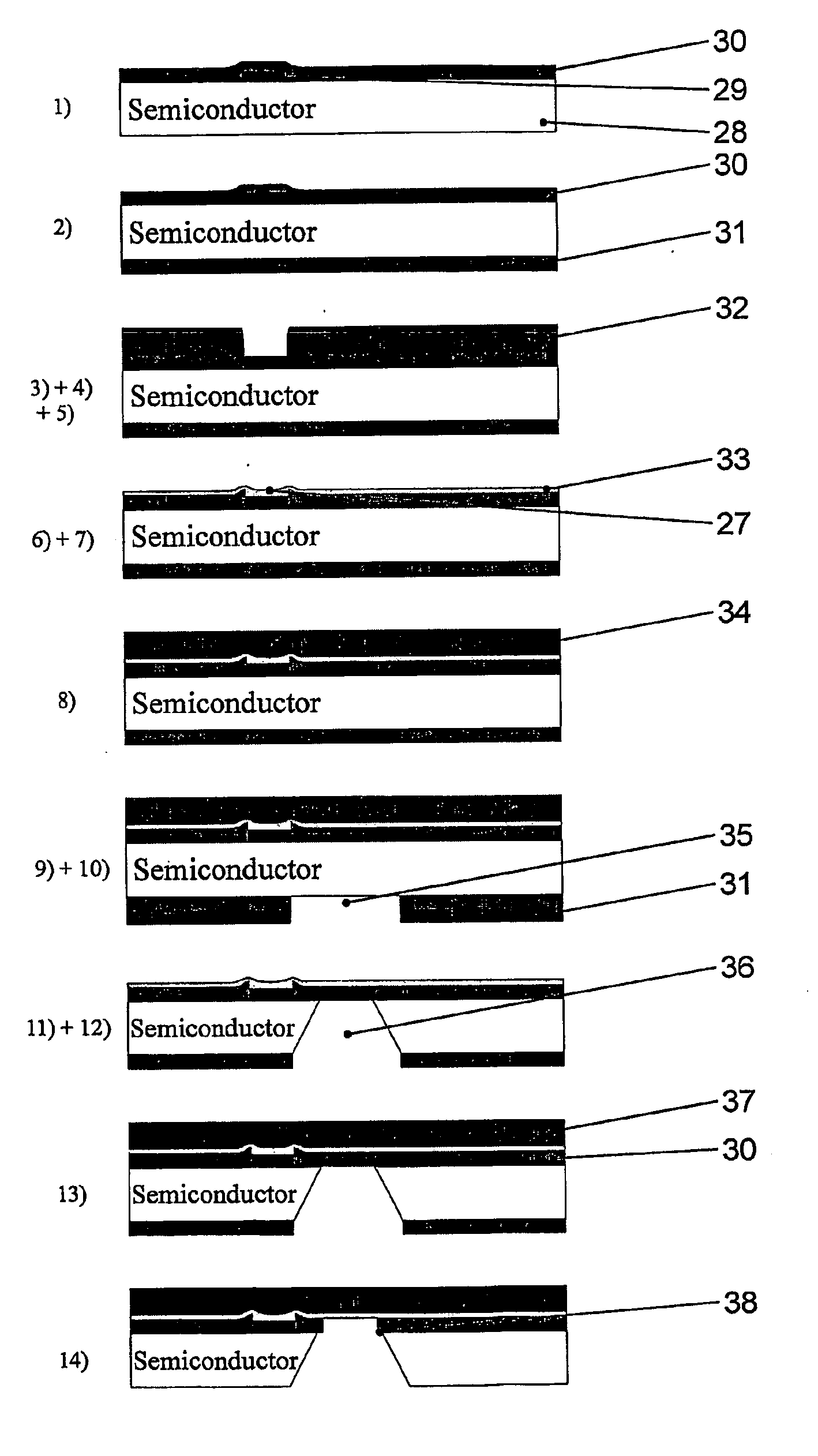
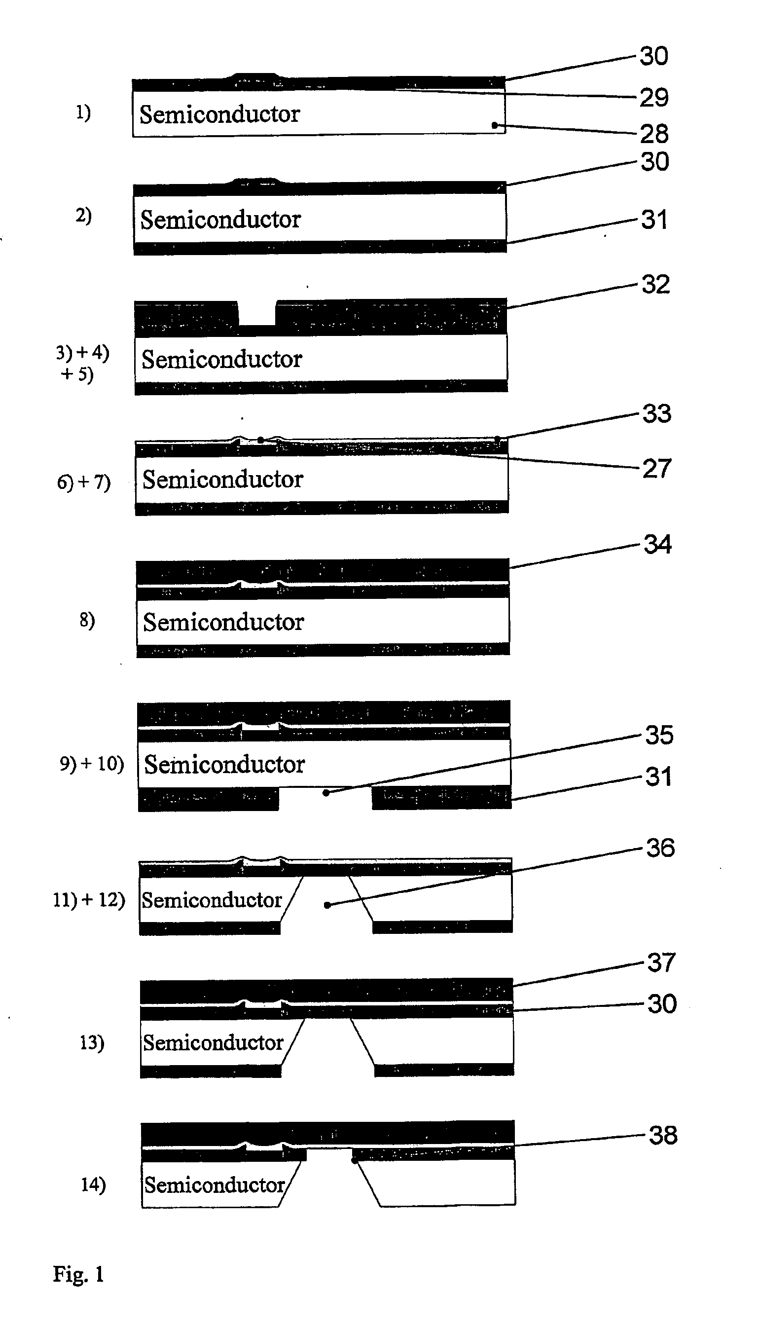
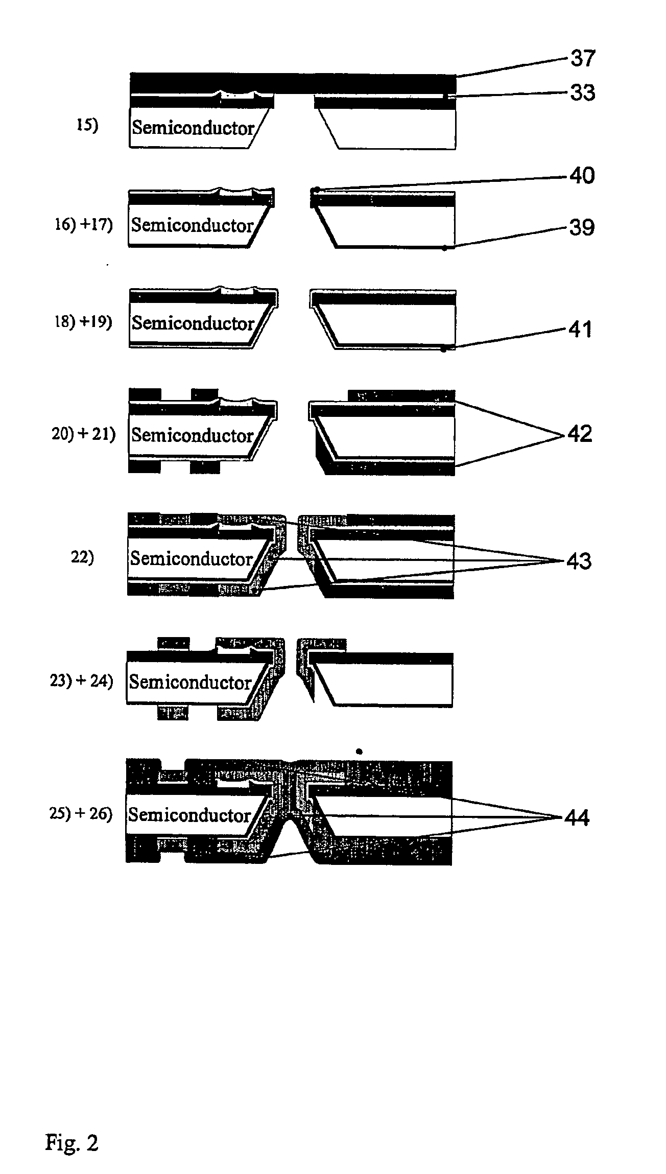
[0036] In the preferred embodiment a silicon wafer 28 is used, but more advanced wafers like silicon on insulator may also be used within the scope of the invention.

1) Deposition of PECVD Nitride 30 on Front Side:

[0037] During processing of the feed-throughs the CMOS wafer is repeatedly placed upside down in wafer holders in various process equipment. Thus, a protective layer is needed on the front side of the wafer in order to avoid mechanical damage of the CMOS surface. Especially the aluminium pads are easily scratched in such handling of the wafer. Furthermore, the sensitive CMOS circuits have to be protected from the etchants used for e.g. etching of the through-holes.

[0038] The protective layer has to be selectively removable with respect to the CMOS passivation layer, i.e. the two layers have to be complementary. In this process a PECVD silicon nitride protection layer 30 has been utilised. In the following process a single electric connections is provided through the for...


PUM


Abstract

The invention concerns a process for generating a feed-through in a semiconductor wafer, which has electric circuitry embedded in a front surface whereby the hole for the feed-through is generated by the combined use of a front side protection layer and a wet KOH etch process etching the hole from the back side of the wafer, where a photomasking process is subsequently used do define the via followed by deposition of the via material.

Description

AREA OF THE INVENTION [0001] The invention concerns a process for generating a feed-through in a semiconductor wafer, which has electric circuitry embedded in a first surface. The embedded circuitry could be a CMOS or similar electronic device. The invention further concerns an amplifier comprising electric circuitry embedded in a first side of a semiconductor wafer and a feed-through from the first to a second side of the semiconductor wafer. BACKGROUND OF THE INVENTION [0002] Amplifiers are produced on wafers and singulated after production. It has been proposed to mount separate electronic components directly on the wafer prior to singulation of the individual amplifiers. This technique is space saving as it becomes possible to omit the printed circuit board, as all components for driving the amplifier can be placed on the surface of the integrated circuit embedded in the silicon wafer. In some cases it is a problem to provide sufficient space also for the bondpads for in / out sig...

Claims


Application Information

Patent Timeline
Patent Type & Authority Applications(United States)
IPC IPC(8): H01L21/306H01L21/768
CPCH01L21/76898H01L21/30608
Inventor RASMUSSEN, FRANK ENGELSKINDHOJ, JORGENPETERSEN, ANDERS ERIK
Owner OTICON
Why Eureka
Try Eureka