Methods for preparing a bonding surface of a semiconductor wafer

a technology of semiconductor wafers and bonding surfaces, applied in semiconductor devices, solid-state devices, decorative arts, etc., can solve problems such as surface blisters, surface rough patches, and detrimental to good bonding, and achieve the effect of increasing bonding energy and increasing bonding energy

Inactive Publication Date: 2005-10-06
S O I TEC SILICON ON INSULATOR THECHNOLOGIES
View PDF5 Cites 16 Cited by
  • Summary
  • Abstract
  • Description
  • Claims
  • Application Information

AI Technical Summary

Benefits of technology

[0007] Presented is a method for preparing an oxidized surface of a first wafer for bonding with a second wafer. The method includes treating the oxidized surface using a solution of NH4OH/H2O2 to increase the bonding energy between the subsequently bonded first and second wafers. The treatment parameters are advantageously chosen to provide etchin...

Problems solved by technology

However, after implementing such chemical treatments the resulting surfaces have rough patches, which can, in some cases, be more significant than that existing prior to treatment.
The presence of isolated particles or contaminants on the surface of the wafers can also be detrimental to good bonding of the wafers when they are found at its ...

Method used


Image

  • Methods for preparing a bonding surface of a semiconductor wafer
  • Methods for preparing a bonding surface of a semiconductor wafer
  • Methods for preparing a bonding surface of a semiconductor wafer

Examples


Embodiment Construction

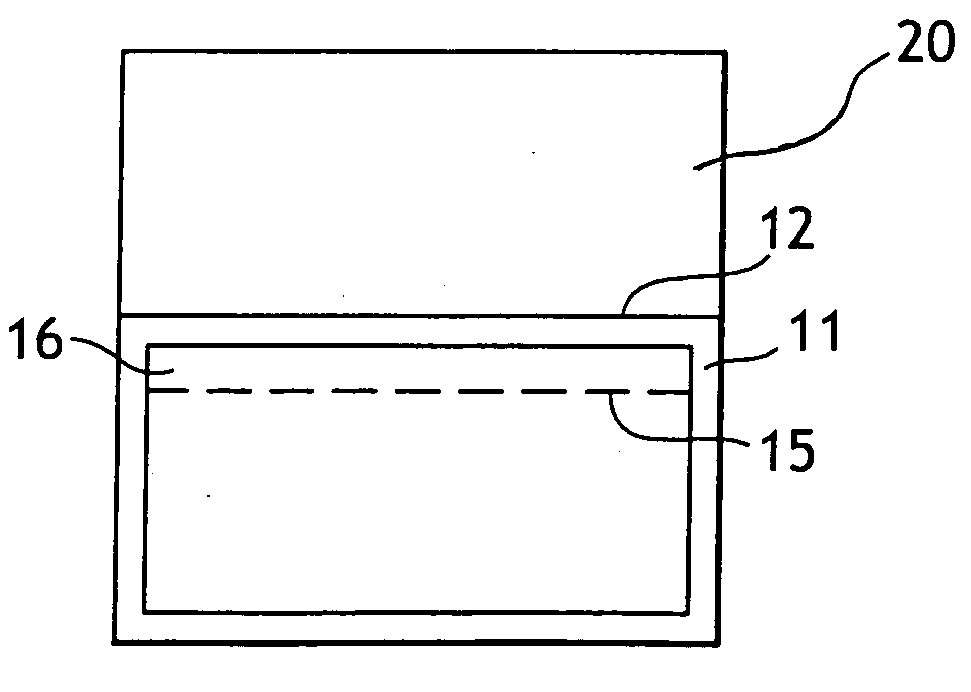
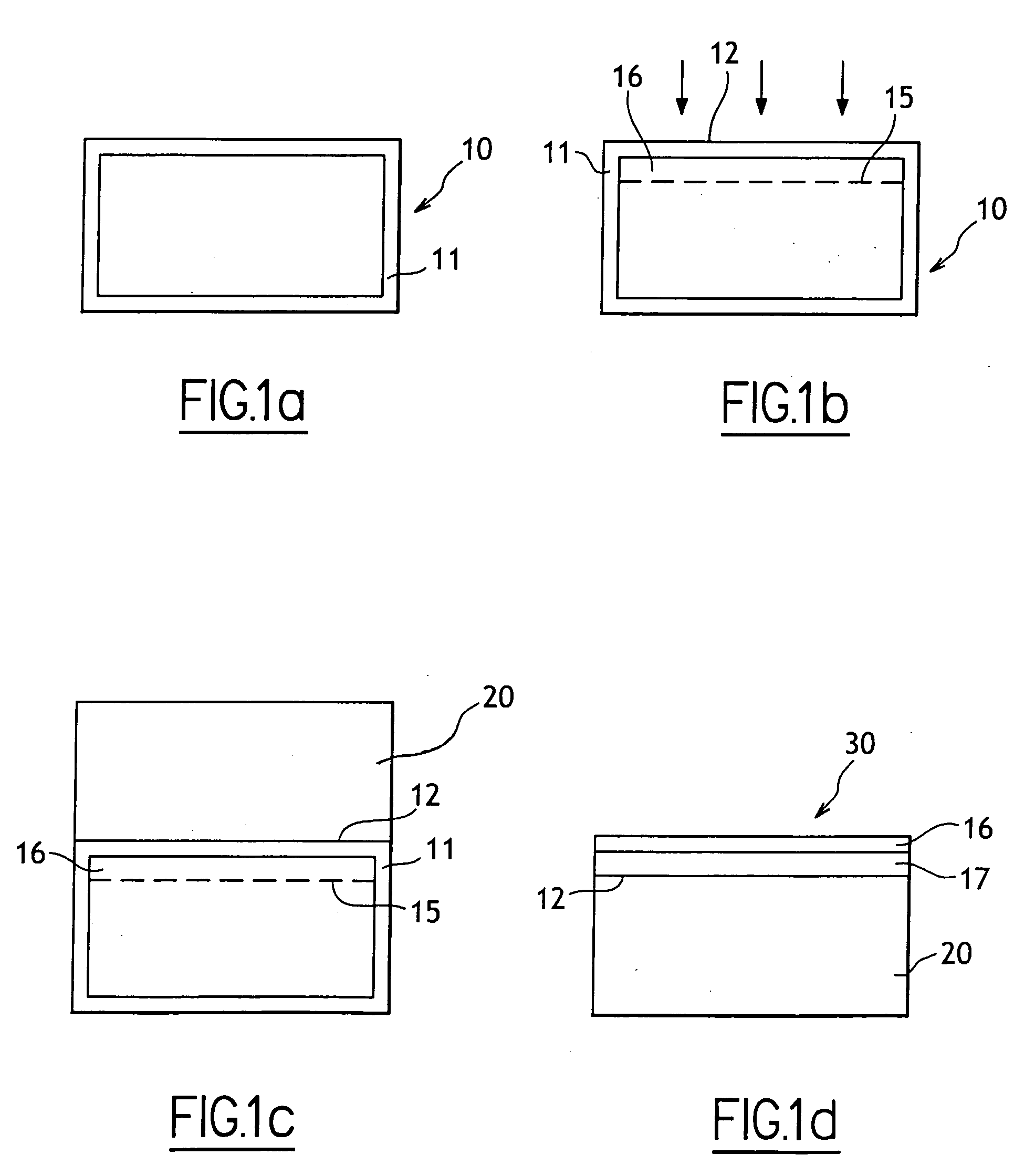
[0018] The wafer cleaning process according to the invention may be used with the thin layer removal method according to the SMART-CUT® process. Referring to FIG. 1a, a first stage includes oxidizing a semi-conductor wafer to create a donor wafer 10 having an oxide layer 11 on its surface. This oxidation process may be native, or may be conducted under a heat treatment (i.e. thermal oxidation), or by deposit of aggregates of SiO2.

[0019] With reference to FIG. 1b, the oxidized donor wafer 10 is subjected to an implantation of atomic species through one of the oxidized surfaces. The atomic species may be hydrogen and / or helium ions. The atomic species used during implantation are dosed and are implanted with a predetermined energy to form a weakened zone 15 at a pre-set depth under the surface of the donor wafer 10. The weakened zone 15 has a particular weakness relative to the rest of the donor wafer 10. A film 16 is thus formed that is delimited by the weakened zone 15 and the oxid...


PUM

PropertyMeasurementUnit
Temperatureaaaaaaaaaa
Diameteraaaaaaaaaa

Abstract

A method for preparing an oxidized surface of a first wafer for bonding with a second wafer. The method includes treating the oxidized surface using a mix of NH4OH/H2O2 to increase the bonding energy between the first and second wafers. The treatment parameters are chosen such that etching occurs that is sufficient to remove isolated particles from the oxidized surface, but that is sufficiently weak to smooth the surface without creating rough patches thereon. Also described is a thin layer removal process, which may advantageously be used to fabricate a semiconductor on insulator structure.

Description

BACKGROUND ART [0001] The present invention generally relates to the bonding of two semiconductor wafers suitable for us in micro-electronics, optics, or optronics applications. In particular, the invention relates to preparing an oxidized bonding surface of at least one of the wafers, wherein treatment parameters are chosen to provide etching that is sufficient to remove isolated particles from the oxidized surface but that is sufficiently weak to smooth the surface without creating rough patches thereon. [0002] Atomic species may be implanted through an oxidized surface of a wafer to form a weakened area therein at a pre-set depth beneath the oxidized surface (thus creating a film on the wafer surface). It is then possible to detach the surface film from the implanted wafer after it has been bonded to another substrate. An example of such a detachment process is the SMART-CUT® process, which is known to skilled person in the art (see “Silicon-on-Insulator Technology, Materials to ...

Claims


Application Information

Patent Timeline
IPC IPC(8): H01L21/306H01L21/762
CPCH01L21/76254H01L21/302H01L27/12
Inventor MALEVILLE, CHRISTOPHEMAUNAND TUSSOT, CORINNE
Owner S O I TEC SILICON ON INSULATOR THECHNOLOGIES
Why Eureka
Try Eureka