Low-stress packaging method of MEMS chip

A packaging method and low-stress technology, which can be used in measurement devices, decorative art, microstructure devices, etc., can solve the problems of low-temperature packaging technology, such as low bonding temperature, low bonding rate, and many holes in the bonding interface, and achieve improved chemical performance. Effects of reactivity, enhanced bonding strength, and increased atomic-scale contact area

Pending Publication Date: 2021-12-07
SHENYANG ACAD OF INSTR SCI
View PDF0 Cites 0 Cited by
  • Summary
  • Abstract
  • Description
  • Claims
  • Application Information

AI Technical Summary

Problems solved by technology

[0004] The bonding temperature of low-temperature packaging technology is low, and it is impossible to realize the viscous flow of SIO2 at high te

Method used


Image

  • Low-stress packaging method of MEMS chip
  • Low-stress packaging method of MEMS chip
  • Low-stress packaging method of MEMS chip

Examples


Embodiment 1

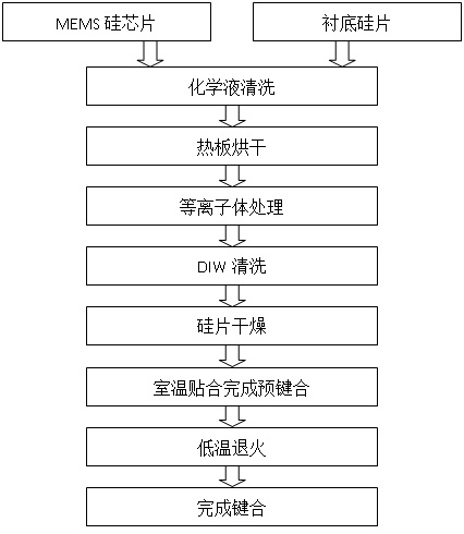
[0054] The invention is a MEMS chip low-stress packaging method, which uses the MEMS silicon chip and substrate silicon chip manufactured by all processes, and sequentially performs chemical liquid treatment, hot plate drying, plasma treatment, DIW (deionized water) cleaning, Silicon wafer drying, pre-bonding, low-temperature annealing and other processes are used to realize low-stress packaging of MEMS chips with homogeneous materials. process such as figure 1 As shown, the specific steps are as follows:

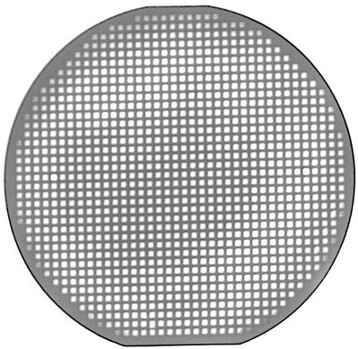
[0055] Step 1. Use double-sided polished silicon wafers, one is the completed MEMS silicon chip, and the other is the substrate silicon wafer, and the micromachining method is used to complete the array through-hole fabrication;

[0056] Step 2, use the SPM solution under the condition of 120°C, the volume ratio is H 2 SO 4 :H 2 o 2 = 5:1 (where H 2 SO 4 The concentration is 96.0±1.0%, H 2 o 2 The concentration is 31.0±1.0%), the surface treatment of the MEMS silicon...

Embodiment 2

[0065] In this embodiment, a double-sided polished silicon wafer is used, one of which is a finished MEMS silicon chip, and the substrate silicon wafer is mechanically drilled to complete the array through-hole fabrication. Except that the process parameters listed in the following steps change, all the other process steps and process parameters are completely consistent with embodiment 1.

[0066] In step 2, use the SPM solution under the condition of 100°C, and the volume ratio is H 2 SO 4 :H 2 o 2 = 10:1 (where H 2 SO 4 The concentration is 96.0±1.0%, H 2 o 2 The concentration is 31.0±1.0%), the MEMS silicon chip and the substrate silicon chip are surface treated, the treatment time is 30min, and the DIW cleaning is 30min;

[0067] In step 3, use the RCA1 solution at 50°C, and the volume ratio is NH 4 OH:H 2 o 2 :H 2 O= 1:1:10 (where NH 4 OH concentration is 28.0~30.0%, H 2 o 2 The concentration is 31.0±1.0%), the MEMS chip and the substrate silicon wafer are ...

Embodiment 3

[0073] In this embodiment, except that the process parameters listed in the following steps are changed, the remaining process steps and process parameters are completely consistent with those of Example 1.

[0074] In step 2, use the SPM solution under the condition of 110°C, and the volume ratio is H 2 SO 4 :H 2 o 2 = 7:1 (where H 2 SO 4 The concentration is 96.0±1.0%, H 2 o 2 Concentration is 31.0±1.0%), surface treatment of MEMS silicon chips and substrate silicon wafers;

[0075] In step 3, use the RCA1 solution at 60°C, and the volume ratio is NH 4 OH:H 2 o 2 :H 2 O= 1:1:7 (where NH 4 OH concentration is 28.0~30.0%, H 2 o 2 The concentration is 31.0±1.0%), the surface treatment of the MEMS silicon chip and the substrate silicon chip is carried out, the treatment time is 20min, and the DIW cleaning is 60min;

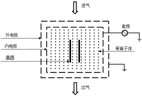
[0076] In step 5, anode voltage 2000V, anode current 800mA, gate current 160mA, processing time 30sec, O 2 Flow 160l / hr, CF 4 Flow 160l / hr;

[0077...


PUM


Abstract

The invention discloses a low-stress packaging method of an MEMS chip, and belongs to the technical field of micromachining. The method comprises the steps: sequentially carrying out chemical liquid treatment, hot plate drying, plasma treatment, DIW cleaning, silicon wafer drying, pre-bonding, low-temperature annealing and other processes on a silicon chip and a substrate silicon wafer, so the MEMS silicon chip homogeneous material low-stress packaging is achieved; wherein the chemical liquid cleaning is mainly characterized in that SPM and RCA1 solutions are used for carrying out surface treatment on the surface of the silicon wafer under specific conditions, so that the silicon wafer has hydrophilicity, and a large number of hydroxyl groups are hung on the silicon wafer; O2 and CF4 mixed gas plasma is used for activating the surface of the chip, and the gas flow direction is parallel to the surface of the silicon wafer for washing treatment, so the surface activation energy is enhanced, the roughness is reduced, and a porous structure which is easy to eliminate interface holes is formed; DIW cleaning and silicon wafer drying are carried out, so that the surface of the silicon wafer is dehydrated and dried, moderate humidity is kept, alkyl suitable for bonding is suspended, and a good surface state is formed; and pre-bonding under specific conditions and step-by-step annealing are carried out, so that low-stress packaging meeting the technical requirements of the MEMS chip is realized.

Description

technical field [0001] The invention belongs to the technical field of micromachining, and specifically relates to a manufacturing method based on single crystal silicon material to realize low-stress packaging of MEMS chip homogeneous material. Background technique [0002] As we all know, chip packaging is an important and key technology in micromachining and manufacturing. It is widely used in the manufacture of three-dimensional microstructures, ICs and MEMS devices. It is an indispensable and key manufacturing technology that determines the performance of MEMS devices. At present, the packaging of silicon-based MEMS chips mostly adopts the microstructure composed of silicon and glass. Since glass and silicon are heterogeneous materials, their characteristics are different. Due to the thermal mismatch of the materials, the packaging stress will inevitably be introduced during the packaging process, which will easily lead to MEMS The performance of the device is degraded...

Claims


Application Information

Patent Timeline
IPC IPC(8): B81C3/00B81C1/00B81B7/00B81B7/02
CPCB81B7/02B81B7/0045B81C1/00285B81C3/004B81C2203/051
Inventor 李颖张治国贾文博李振波祝永峰任向阳叶挺徐长伍关维冰白雪松尹萍海腾
Owner SHENYANG ACAD OF INSTR SCI
Why Eureka
Try Eureka