Stress-relief layer and stress-compensation collar in contact arrays, and processes of making same

a stress-relief layer and stress-compensation collar technology, applied in the direction of stress/warp reduction, printed circuits, sustainable manufacturing/processing, etc., can solve the problems of thermal expansion-mismatch challenges, and the size of smaller balls posing an increasing challenge to solder joint performan

Inactive Publication Date: 2005-10-06
INTEL CORP
View PDF4 Cites 12 Cited by
  • Summary
  • Abstract
  • Description
  • Claims
  • Application Information

AI Technical Summary

Problems solved by technology

Thermal expansion-mismatch challenges exist between the die, the underfill material, and the substrate to which the die is mounted and to connect

Method used


Image

  • Stress-relief layer and stress-compensation collar in contact arrays, and processes of making same
  • Stress-relief layer and stress-compensation collar in contact arrays, and processes of making same
  • Stress-relief layer and stress-compensation collar in contact arrays, and processes of making same

Examples


Embodiment Construction

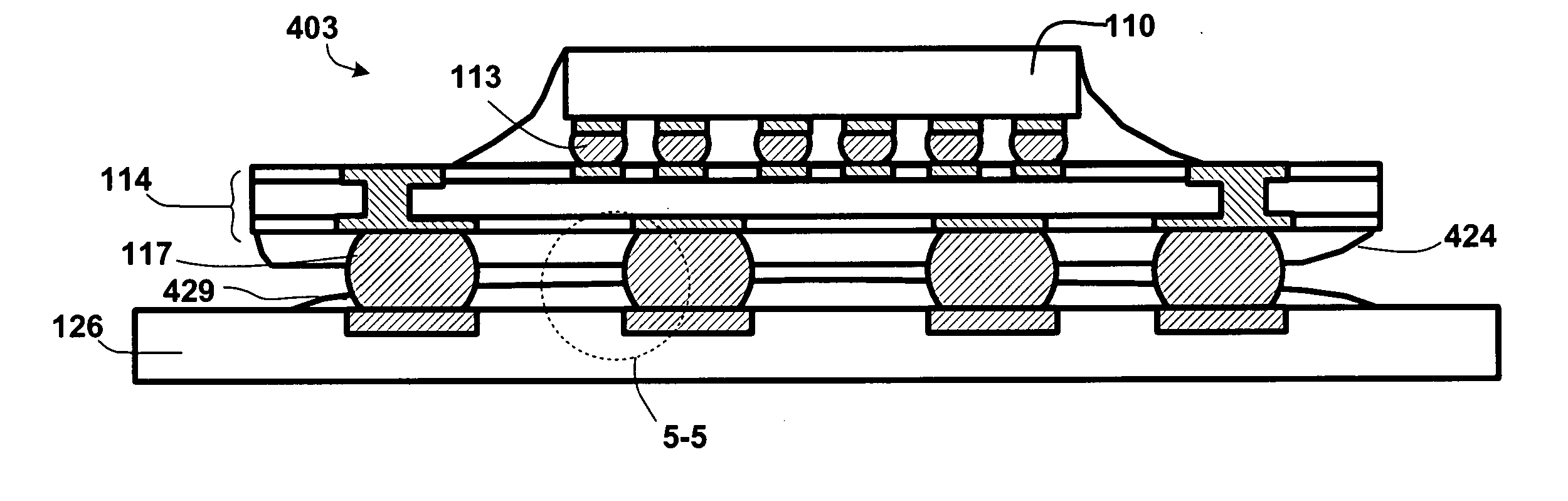
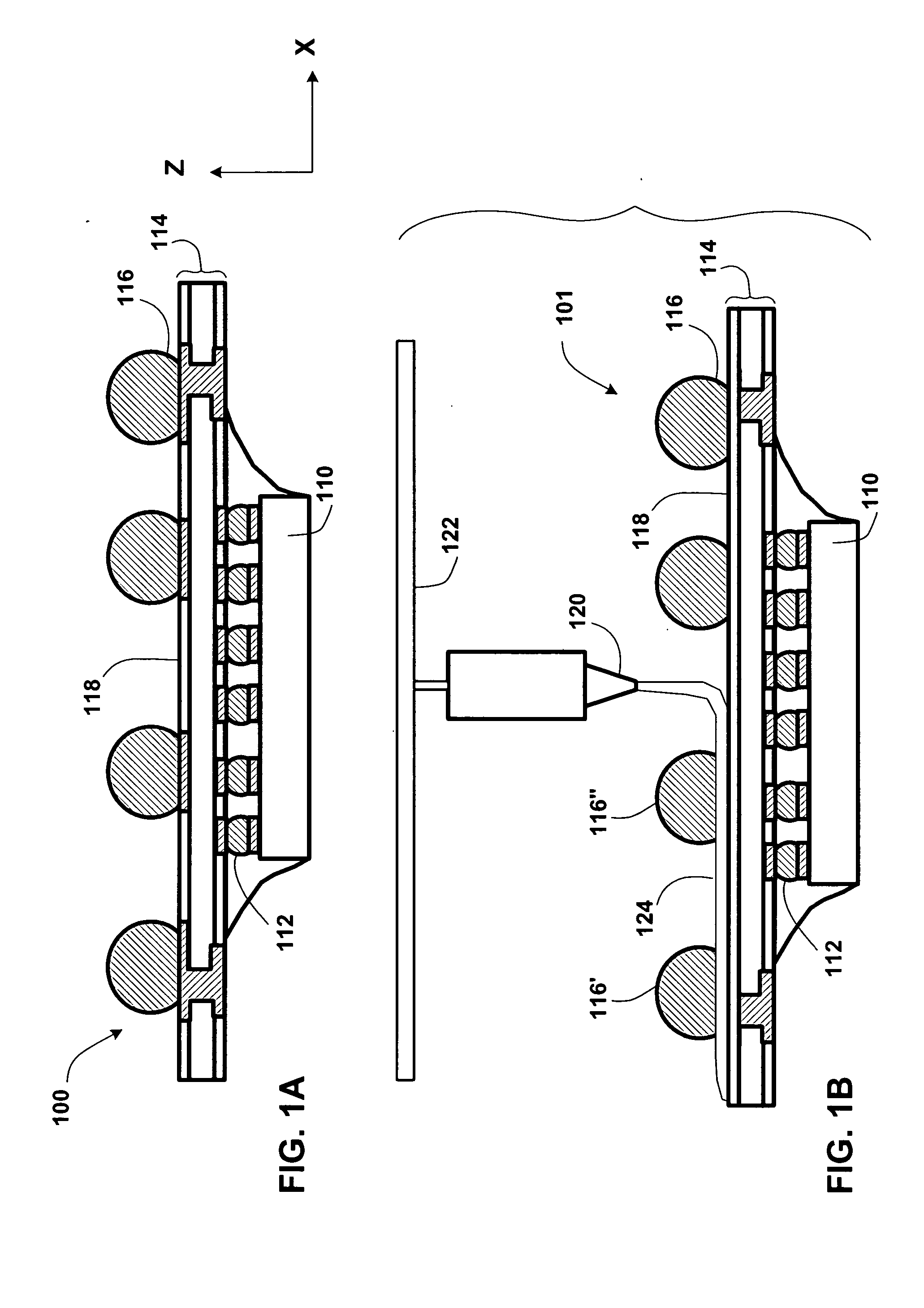
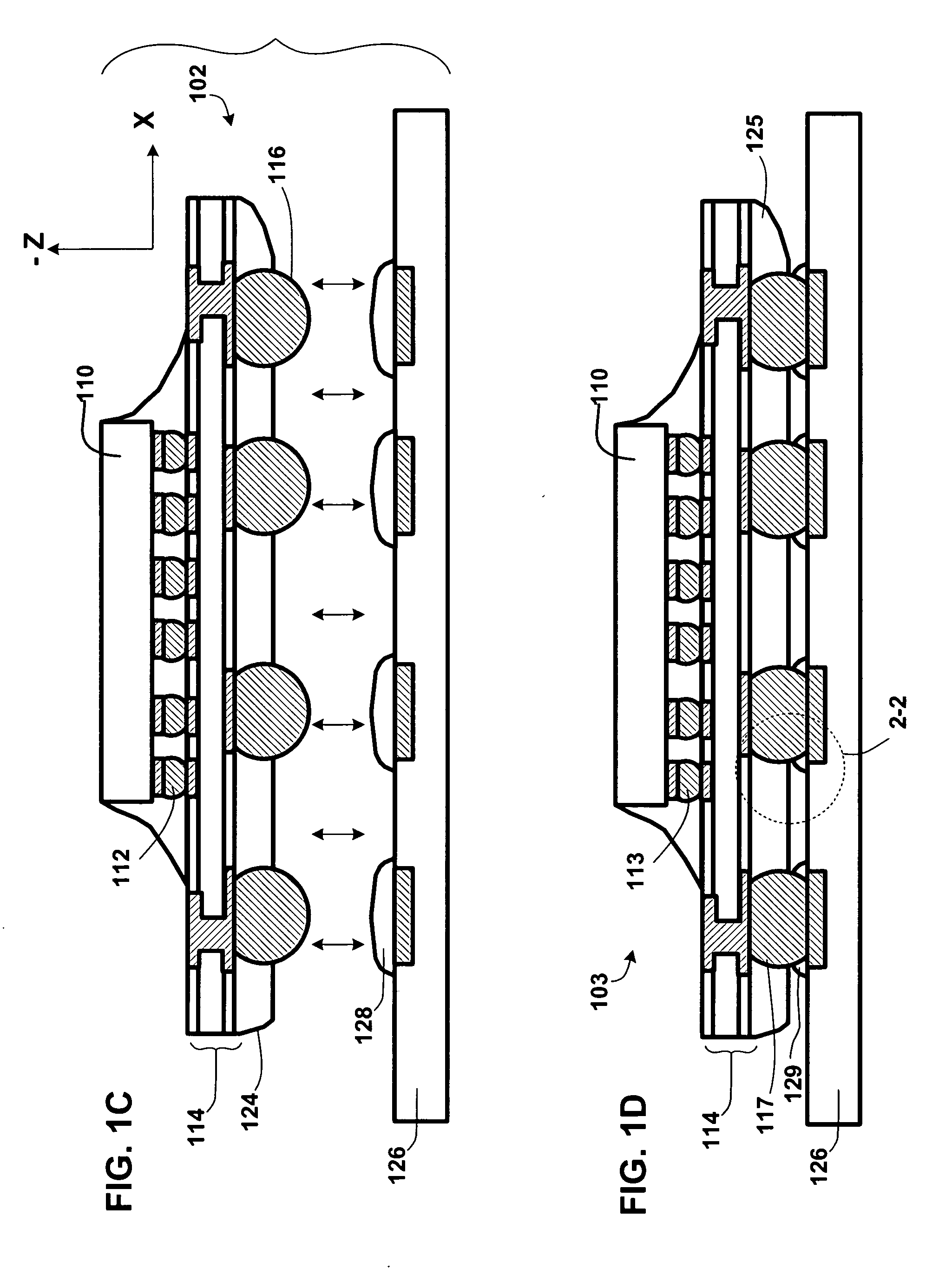
[0023] The following description includes terms, such as upper, lower, first, second, etc. that are used for descriptive purposes only and are not to be construed as limiting. The embodiments of a device or article described herein can be manufactured, used, or shipped in a number of positions and orientations. The terms “die” or “processor” generally refer to the physical object that is the basic workpiece that is transformed by various process operations into the desired integrated circuit device. A board is typically a conductor-overlay structure that is insulated and that acts as a mounting substrate for the die. A board is usually singulated from a board array. A die is usually singulated from a wafer, and wafers may be made of semiconducting, non-semiconducting, or combinations of semiconducting and non-semiconducting materials.

[0024] A “solder bump” and “electrical bump” is understood to be a unit of electrically conductive material such as a tin-lead solder, a tin-indium so...


PUM


Abstract

A stress-relief layer is formed by dispensing a polymer upon a substrate lower surface under conditions to partially embed a solder bump that is disposed upon the lower surface. The stress-relief layer flows against the solder bump. A stress-compensation collar is formed on a board to which the substrate is mated and the SCC partially embeds the solder bump. An article that exhibits a stress-relief layer and a stress-compensation collar is also included. A computing system that includes a stress-relief layer and a stress-compensation collar is also included.

Description

TECHNICAL FIELD [0001] Disclosed embodiments relate to a stress-relief layer and a stress-compensation collar in a microelectronic device package. BACKGROUND INFORMATION [0002] Chip packaging is often intensely involved with heat removal. Thermal expansion-mismatch challenges exist between the die, the underfill material, and the substrate to which the die is mounted and to connecting structures such as the motherboard. The thermal mismatch often is exhibited at the joint of a solder bump and its bond pad. [0003] One method of dealing with solder bump stress on a motherboard is to encapsulate the solder bumps at the corners with an underfill layer. This method only encapsulates solder bumps at the periphery of the package. It does not encapsulate the solder bumps at the center. [0004] Future packaging technology especially in the chipset application, will drive finer pitch as package size shrinks. With miniaturization of pitch, smaller ball size poses an increasing challenge to sold...

Claims


Application Information

Patent Timeline
IPC IPC(8): H01L21/44H01L23/498H05K1/02H05K3/34
CPCH01L23/49816H01L23/49838H01L2224/16H01L2924/01077H01L2924/15311H05K1/0271H05K3/3436H05K2201/10977H05K2203/0126H05K2203/1189Y02P70/613H01L2224/05573H01L2224/05568H01L2924/00014H01L2224/05599H01L2224/06131Y02P70/50
Inventor SUH, DAEWOONGJAYARAMAN, SAIKUMARBIN BASIRON, MOHD ERWAN P.LIM, SHEAU HOOIP. CHIN, YOONG TATT
Owner INTEL CORP
Why Eureka
Try Eureka