Semiconductor device and method of fabricating the same

Inactive Publication Date: 2005-10-06
KK TOSHIBA
View PDF5 Cites 22 Cited by
  • Summary
  • Abstract
  • Description
  • Claims
  • Application Information

AI Technical Summary

Benefits of technology

[0011] Therefore, an object of the present invention is to provide a semiconductor device in which a desirable trench fill capability of the insulating

Problems solved by technology

As a result, the trench cannot completely be filled with the insulating film material, whereupon voids are formed in the trench.
The voids further result in a new failure such as short circuit between the elements with an increasing frequency of occurrence.
However, this method has the following inconvenience.
Accordingly, limitations of a lower limit value of the taper angle beco

Method used


Image

  • Semiconductor device and method of fabricating the same
  • Semiconductor device and method of fabricating the same
  • Semiconductor device and method of fabricating the same

Examples


Embodiment Construction

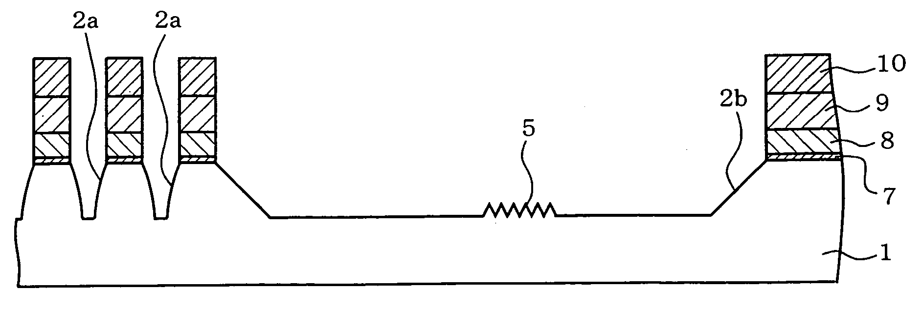
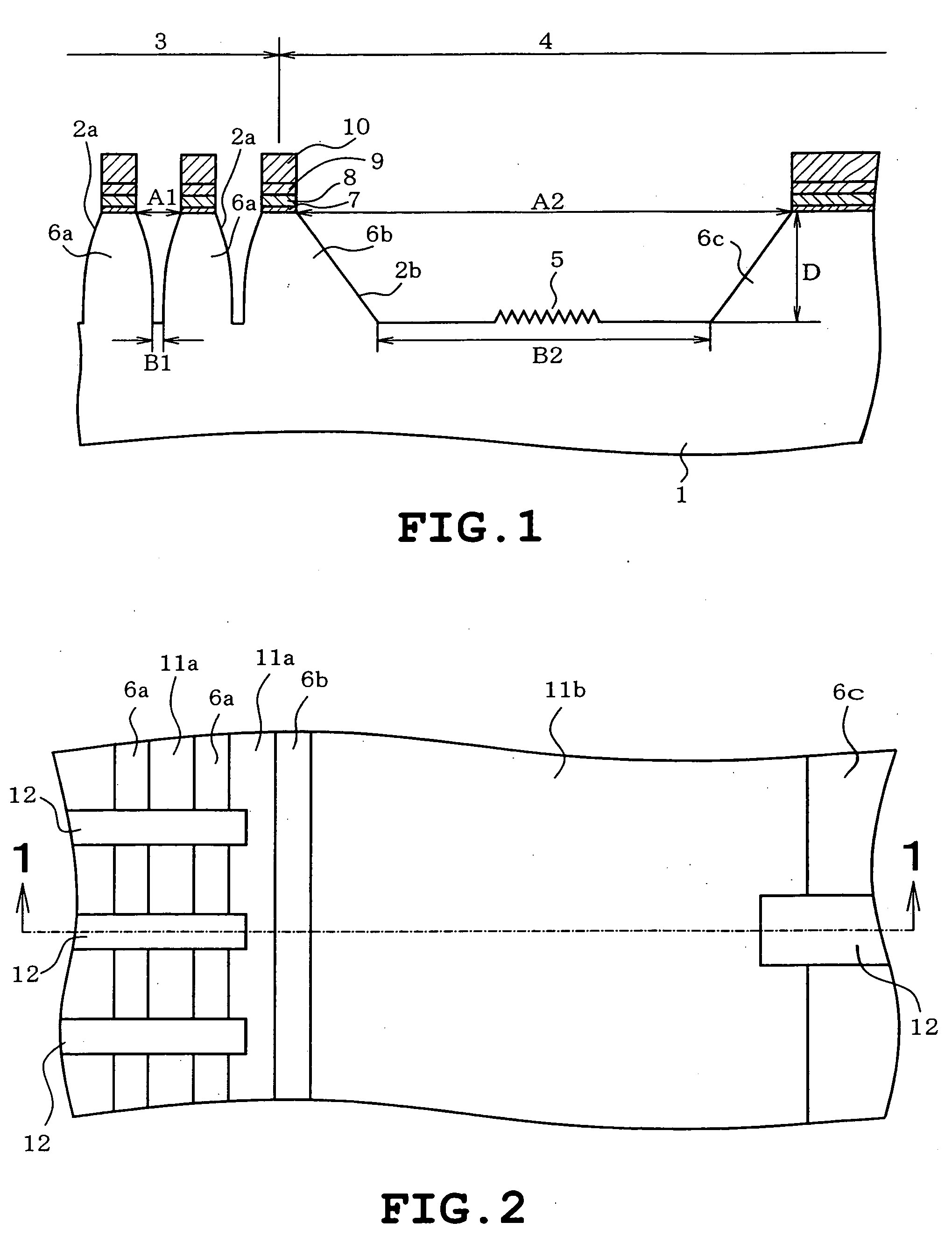
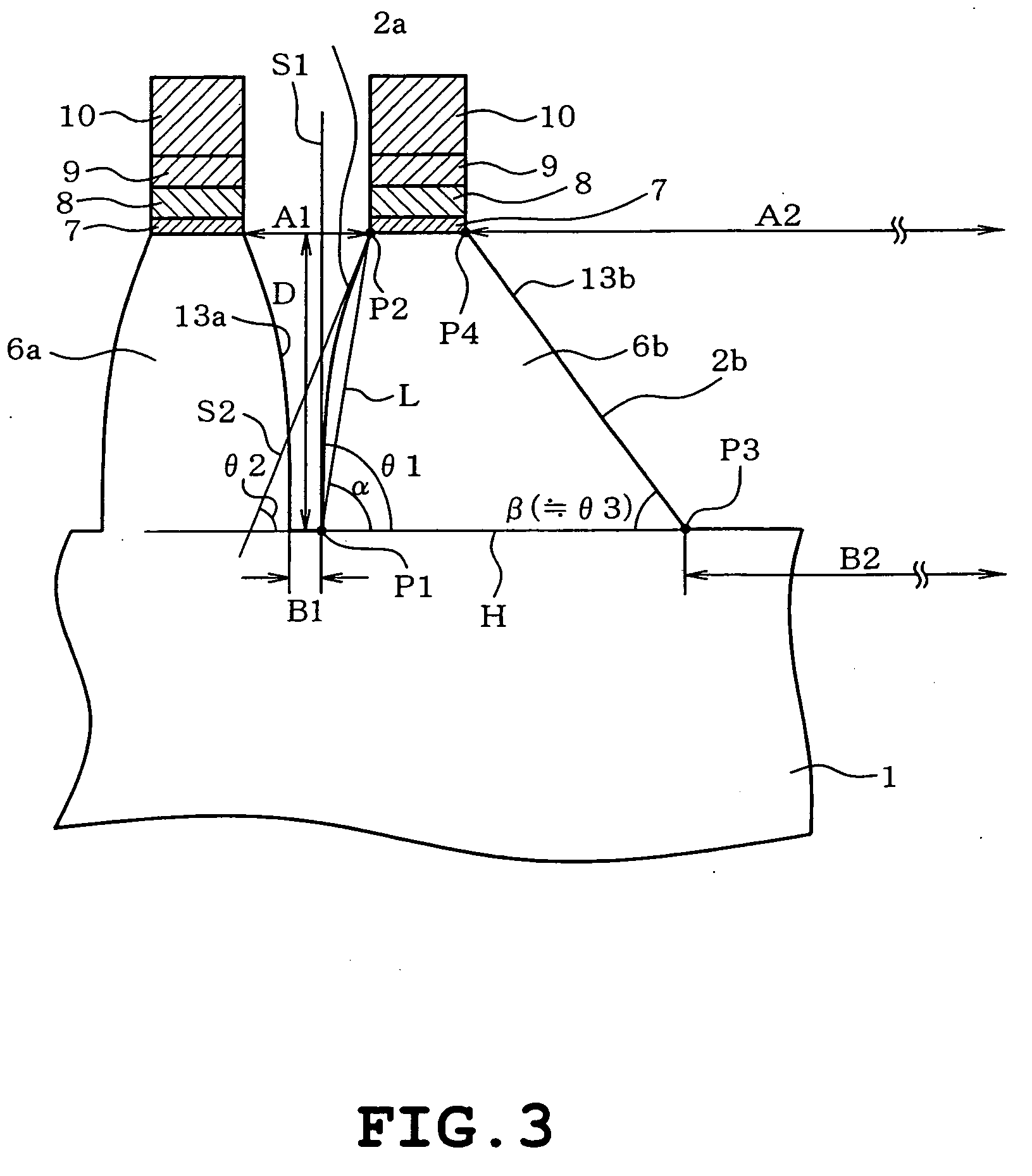
[0023] One embodiment of the present invention will be described with reference to the accompanying drawings. The invention is applied to a flash memory which is one type of non-volatile memory. Referring to FIG. 1, the state of the semiconductor device after execution of a trench forming process is shown. FIG. 2 shows a control gate electrode. FIG. 1 is a sectional view taken along line 1-1 in FIG. 2. Chips composing the flash memory each include a memory cell region in which a number of memory cells are formed and a peripheral circuit region in which peripheral circuits for driving the memory cells are formed.

[0024] A silicon substrate 1 serving as a semiconductor substrate has trenches 2a and 2b for forming element isolation regions. The trenches 2a and 2b have opening widths A1 and A2 respectively and the same depth D as each other. The trench 2a has a higher aspect ratio R1 (D / A1) so as to correspond to a memory cell region 3, whereas the trench 2b has a lower aspect ratio R2 ...


PUM


Abstract

A semiconductor device includes a semiconductor substrate and first and second trenches. The first trench with a high aspect ratio is formed in a surface of the semiconductor substrate and has a bottom, two sidewalls and an open end. The first trench is formed so that at the bottom side, an inclination of each sidewall relative to the bottom has a first angle approximate to a right angle and at the bottom side, the inclination of each sidewall relative to the bottom has a second angle smaller than the first angle. The second trench has a lower aspect ratio than the first trench. The second trench has a bottom, two sidewalls and an open end and is formed so that an inclination of each sidewall relative to the bottom is substantially uniform from the bottom side to the open end side and has a third angle which is approximate to the second angle.

Description

CROSS-REFERENCE TO RELATED APPLICATION [0001] This application claims priority from Japanese patent application No. 2004-85051, filed Mar. 23, 2004, the content of which is incorporated herein by reference. BACKGROUND OF THE INVENTION [0002] 1. Field of the Invention [0003] The present invention relates to a semiconductor device provided with trenches having high and low aspect ratios respectively and a method of fabricating the same. [0004] 2. Description of the Related Art [0005] Semiconductor devices employ a shallow trench isolation (STI) structure in order that elements may be isolated from each other. A trench is formed in a semiconductor substrate and filled with an insulating material such as silicon oxide (SiO2), whereby the element isolating STI structure is formed. [0006] In forming a trench, a semiconductor substrate with an etching pattern is disposed in a vacuum process chamber of a processing apparatus. A reactive gas is then introduced into the chamber and a discharg...

Claims


Application Information

Patent Timeline
IPC IPC(8): H01L29/788H01L21/8247H01L21/762H01L21/76H01L27/115H01L29/792H01L21/3065
CPCH01L21/76229H01L21/76232H01L21/762
Inventor MATSUMOTO, TAKANORI
Owner KK TOSHIBA
Why Eureka
Try Eureka