Substrate susceptors for receiving semiconductor substrates to be deposited upon and methods of depositing materials over semiconductor substrates

a technology of substrate susceptors and semiconductor substrates, which is applied in the direction of solid-state diffusion coating, crystal growth process, polycrystalline material growth, etc., can solve the problems of poor selective silicon deposition repeatability, difficult control of substrate temperature, and less controlled or uniform deposition over substrates

Inactive Publication Date: 2005-10-13
MICRON TECH INC
View PDF20 Cites 456 Cited by
  • Summary
  • Abstract
  • Description
  • Claims
  • Application Information

AI Technical Summary

Benefits of technology

[0024] In one implementation, a method of depositing material over a semiconductor substrate comprises positioning a semiconductor substrate on a substrate bearing surface of a susceptor. The bearing surface comprises at least one vacuum opening therein. A vacuum force is applied to the at least one opening effective to apply a pulling force on the semiconductor substrate against the bearing surface. While the vacuum force is applied, the susceptor is rotated while depositing a material over the semiconductor substrate.
[0025] In one implementation, a substrate susceptor for receiving a semiconductor substrate to be deposited upon comprises a body having a front substrate receiving side, a back side, and a peripheral edge. A surface is on the front substrate receiving side over which at least a portion of a semiconductor substrate to be deposited upon is to be received. The surface comprises at least three gas emitting openings configured to apply a substrate levitating and rotating force from gas emitted from the openings effective to levitate and rotate said semiconductor substrate relative to the susceptor body.
[0026] In one implementation, a method of depositing material over a semiconductor substrate comprises positioning a semiconductor substrate over a surface of a susceptor. The surface comprises at least three gas emitting openings therein. Gas is emitted from the at least three openings effective to levitate and rotate the semiconductor substrate relative to the susceptor. While levitating and rotating the semiconductor substrate relative to the susceptor, a material is deposited over the semiconductor substrate.

Problems solved by technology

Such can further result in temperature variation across the substrate and, regardless, result in less controlled or uniform deposition over substrate 14.
Unfortunately, a selective epitaxial silicon process such as described above will also deposit upon silicon carbide in addition to elemental form silicon.
This is undesirable at least for purposes of temperature control of the substrate during deposition.
Therefore as a silicon coating builds upon the back side of the susceptor, more energy is typically added to the heat lamps which undesirably increases the substrate temperature in a manner which is difficult to control.
Yet without re-establishing the chamber to a similar baseline condition, wafer repeatability in the selective silicon deposition is poor.

Method used


Image

  • Substrate susceptors for receiving semiconductor substrates to be deposited upon and methods of depositing materials over semiconductor substrates
  • Substrate susceptors for receiving semiconductor substrates to be deposited upon and methods of depositing materials over semiconductor substrates
  • Substrate susceptors for receiving semiconductor substrates to be deposited upon and methods of depositing materials over semiconductor substrates

Examples


Embodiment Construction

[0056] This disclosure of the invention is submitted in furtherance of the constitutional purposes of the U.S. Patent Laws “to promote the progress of science and useful arts” (Article 1, Section 8).

[0057] The invention comprises structural and methodical aspects, neither of which is limited by the other unless literal limiting language thereto appears in a claim under analysis.

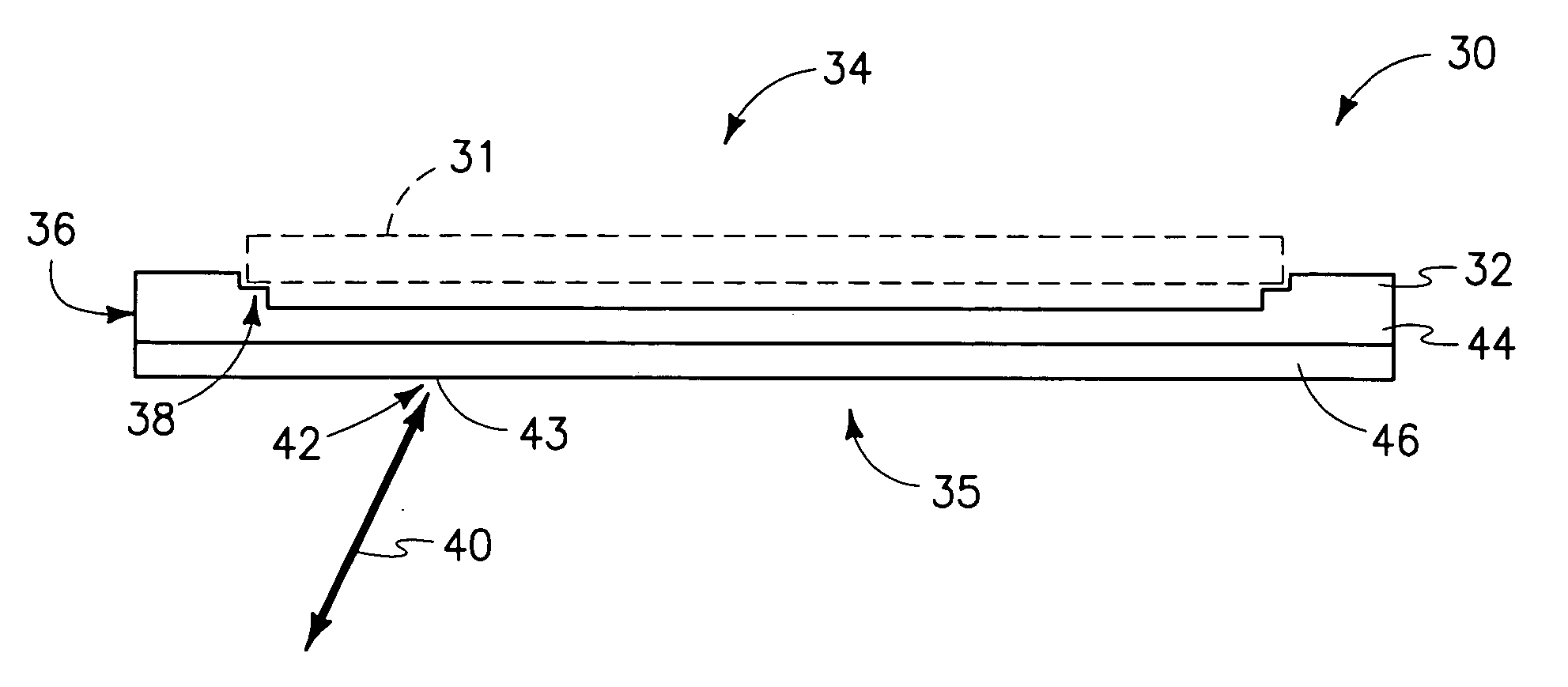
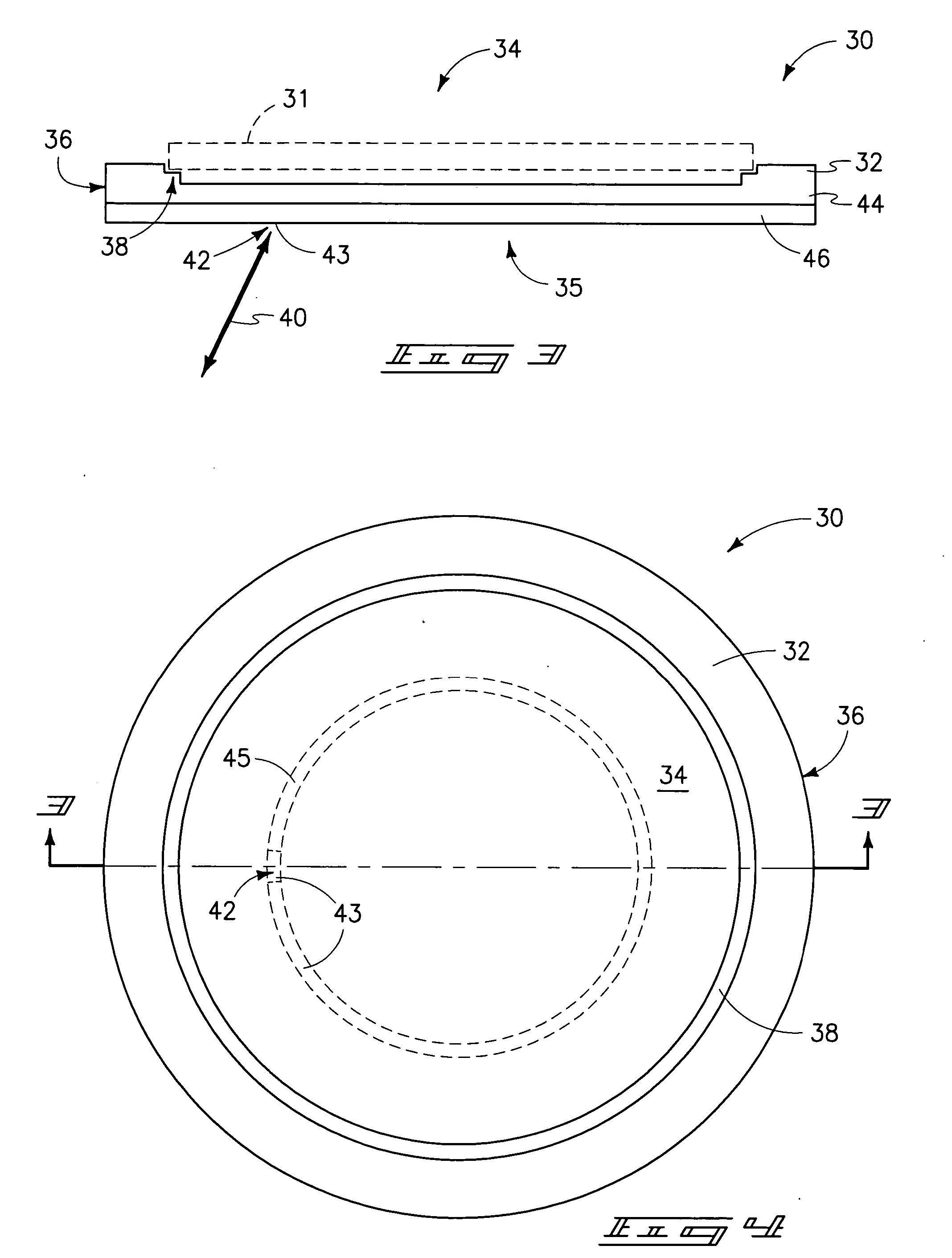
[0058] Certain aspects of the invention are initially described with reference to FIGS. 3-6. Referring initially to FIGS. 3 and 4, a substrate susceptor for receiving a semiconductor substrate for selective epitaxial silicon-comprising depositing thereon is indicated generally with reference numeral 30. Such depositing will comprise measuring the emissivity of the susceptor from at least one susceptor location in a non-contacting manner, for example and by way of example only, by optical pyrometry using an infrared sensor. Susceptor 30 comprises a body 32 having a front substrate receiving side 34, a back s...


PUM

PropertyMeasurementUnit
temperatureaaaaaaaaaa
pressureaaaaaaaaaa

Abstract

In one implementation, a substrate susceptor for receiving a semiconductor substrate for selective epitaxial silicon-comprising depositing thereon, where the depositing comprises measuring emissivity of the susceptor from at least one susceptor location in a non-contacting manner, includes a body having a front substrate receiving side, a back side, and a peripheral edge. At least one susceptor location from which emissivity is to be measured is received on at least one of the front substrate receiving side, the back side, and the edge. Such at least one susceptor location comprises an outermost surface comprising a material upon which selective epitaxial silicon will not deposit upon during selective epitaxial silicon depositing on a semiconductor substrate received by the susceptor for at least an initial thickness of epitaxial silicon depositing on said substrate. Other aspects and implementations are contemplated.

Description

TECHNICAL FIELD [0001] This invention relates to substrate susceptors for receiving semiconductor substrates to be deposited upon and to methods of depositing materials over semiconductor substrates. BACKGROUND OF THE INVENTION [0002] Integrated circuitry fabrication includes deposition of material and layers over a substrate. One or more substrates are received within a deposition chamber within which deposition typically occurs. One or more precursors or substances are caused to flow to the substrate, typically as a vapor, to effect deposition of a layer over the substrate. A single substrate is typically positioned or supported for deposition by a susceptor. In the context of this document, a “susceptor” is any device which holds or supports at least one wafer within a chamber or environment for deposition. Deposition may occur by chemical vapor deposition, atomic layer deposition and / or by other means. [0003]FIGS. 1 and 2 diagrammatically depict a prior art susceptor 10, and iss...

Claims


Application Information

Patent Timeline
Patent Type & Authority Applications(United States)
IPC IPC(8): C23C8/00C23C14/50C23C14/54C23C16/00C23C16/458C23C16/48C23C16/52C30B25/02C30B29/06
CPCC23C14/505C23C14/541C23C16/45521C23C16/4584C23C16/481C23C16/52C30B25/02C30B29/06
Inventor BLOMILEY, ERIC R.RAMASWAMY, NIRMALDANDO, ROSS S.DREWES, JOEL A.DYNKA, DANNY
Owner MICRON TECH INC
Why Eureka
Try Eureka