Doping method and manufacturing method for a semiconductor device

a manufacturing method and semiconductor technology, applied in the field of doping methods, can solve the problems of difficult to activate difficult to form a shallow impurity diffusion region having a high concentration of impurities on the semiconductor substrate, and difficult to form a shallow impurity diffusion region having low resistance and high concentration of activated impurities

Active Publication Date: 2005-10-13
KIOXIA CORP
View PDF15 Cites 36 Cited by
  • Summary
  • Abstract
  • Description
  • Claims
  • Application Information

AI Technical Summary

Problems solved by technology

As a result, it is impossible to form a shallow impurity diffusion region having a high concentration of impurities on the semiconductor substrate.
Also, it becomes difficult to activate a high concentration of impurities if the temperature of the RTA process is decreased in order to control the diffusion of the impurities.
Because of such difficulties it is difficult to form a shallow impurity diffusion region having low resistance and a high concentration of activated impurities.
However, in a flash lamp annealing method, there is a problem of a decrease in thermal efficiency due to light of the flash lamp being reflected off of the surface of a semiconductor substrate.
Because of this drop in thermal efficiency, it is impossible to sufficiently activate impurities.
Semiconductor devices have various materials arranged in fine patterns that are often uneven and irregular.
Thus, incident flash lamp light is refracted and light interfere occurs inside the semiconductor substrate.
In a case in which irradiation energy density of flash lamp light is large, there is a concern that hot spots may be formed.
However, crystal defects caused by ion implantation of group IV element will remain after activation annealing.
Therefore, ion implantation of group IV element may be a cause for increasing leakage current of a pn junction, and off-state current of a transistor.
Thus, in current flash lamp annealing methods, although it may be possible to form an impurity diffusion layer having a shallow pn junction, it is difficult to form a low resistance diffused layer having no crystal defects.

Method used


Image

  • Doping method and manufacturing method for a semiconductor device
  • Doping method and manufacturing method for a semiconductor device
  • Doping method and manufacturing method for a semiconductor device

Examples


Embodiment Construction

[0025] Various embodiments of the present invention will be described with reference to the accompanying drawings. It is to be noted that the same or similar reference numerals are applied to the same or similar parts and elements throughout the drawings, and the description of the same or similar parts and elements will be omitted or simplified.

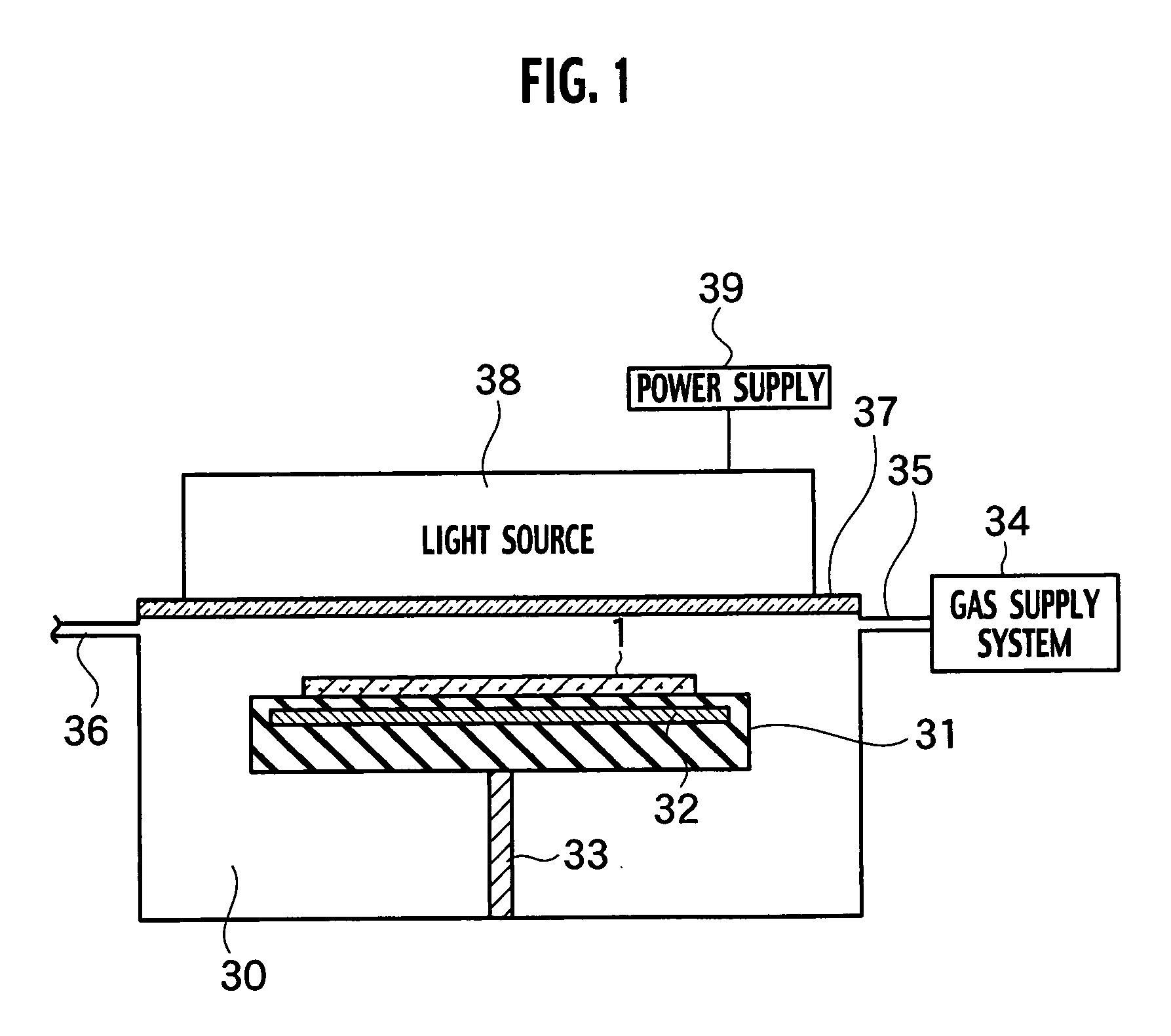
[0026] An annealing apparatus according to an embodiment of the present invention, as shown in FIG. 1, includes a processing chamber 30, a susceptor 31, an intake pipe 35, an exhaust pipe 36, a transparent window 37, and a light source 38. An annealing process is performed in the processing chamber 30 to activate impurity ions implanted into a semiconductor substrate 1, such as Si. The semiconductor substrate 1 is placed on top of the susceptor 31 which is disposed inside of the processing chamber 30. The intake pipe 35 feeds an ambient gas to the processing chamber 30. The exhaust pipe 36 vents the ambient gas from the processing chamber 3...


PUM


Abstract

A doping method includes implanting first impurity ions into a semiconductor substrate, so as to form a damaged region in the vicinity of a surface of the semiconductor substrate, the first impurity ions not contributing to electric conductivity; implanting second impurity ions into the semiconductor substrate through the damaged region, the second impurity ions having an atomic weight larger than the first impurity ions and contributing to the electric conductivity; and heating the surface of the semiconductor substrate with a light having a pulse width of about 0.1 ms to about 100 ms, so as to activate the second impurity ions.

Description

CROSS REFERENCE TO RELATED APPLICATIONS AND INCORPORATION BY REFERENCE [0001] This application is based upon and claims the benefit of priority from prior Japanese Patent Application P2004-111368 filed on Apr. 5, 2004; the entire contents of which are incorporated by reference herein. BACKGROUND OF THE INVENTION [0002] 1. Field of the Invention [0003] The present invention relates to a doping method, and particularly to a doping method by annealing with a high intensity light source, and a manufacturing method for a semiconductor device. [0004] 2. Description of the Related Art [0005] It is possible to achieve improvements in a semiconductor device performance of a large scale integration (LSI) and the like by increasing integration, or to put it more plainly, by miniaturization of the elements that build up a semiconductor device. Thus, LSIs are increasingly large-scale while miniaturization of elements such as metal-oxide-semiconductor (MOS) transistors is being taken to a whole n...

Claims


Application Information

Patent Timeline
Patent Type & Authority Applications(United States)
IPC IPC(8): H01L21/336H01L21/425H01L21/8238
CPCH01L21/823814H01L21/2236Y10S438/918Y10S438/964
Inventor ITO, TAKAYUKISUGURO, KYOICHI
Owner KIOXIA CORP
Why Eureka
Try Eureka