Plating apparatus and method

a technology of plating apparatus and substrate, applied in the direction of liquid/solution decomposition chemical coating, coating, electrolysis components, etc., can solve the problems of large plating resolution and definition errors, affecting the stability of the substrate, so as to minimize the risks of damage in plating small, expensive substrates, and reduce the volume required for plating

Inactive Publication Date: 2005-10-20
SURFECT TECH
View PDF81 Cites 13 Cited by
  • Summary
  • Abstract
  • Description
  • Claims
  • Application Information

AI Technical Summary

Benefits of technology

[0050] A primary advantage of the present invention is the ability to finely control the plating processes with regard to, but not limited to, initiation rates, deposition rates, temperature control, and pressure control.
[0051] Another advantage of the present invention is the ability to reduce the volumes required for plating.
[0052] Another advantage of the present invention is the ability to minimize the risks of damage in plating small, expensive substrates and thus reduce the costs inherent in such damage.
[0053] Other objects, advantages and novel features, and further scope of applicability of the present invention are set forth in part in the detailed description to follow, taken in conjunction with the accompanying drawings, and in part will become apparent to those skilled

Problems solved by technology

However, it is difficult to control spurious and extraneous metal deposition onto surface areas where the metal is not desired.
At micron and submicron feature sizes, the magnitude of plating resolution and definition errors can approach, and even exceed, the feature separation distance.
This can cause conductor bridging and electrical shorting of the wafer or substrate.
However, the addition of inhibitors can negatively impact the utility of plating for subsequent joining/connecting procedures.
This effect has discouraged the wide use of conventional electroless plating technology for wafer scale electronic joining applications.
The requirement to physically move the wafer or substrate from tank to tank creates a significant risk of damage to the wafer.
The risk of damage is increased by the ongoing trend in the semiconductor processing industry to “thin” wafers by chemical or mechanical means, making an already delicate structure even more fragile.
With respect to the electrolytic plating of thin wafers such as those found in the semiconductor industry, the existing electrolytic plating methodology suffers from certain limitations.
Such build-up detrimentally fuses the contact point to the surface of the wafer and at the completion of the process can result in a tearing or removal of the deposited film at the contact point.
Another limitation of electrolytic plating is that the resulting

Method used


Image

  • Plating apparatus and method
  • Plating apparatus and method
  • Plating apparatus and method

Examples


Embodiment Construction

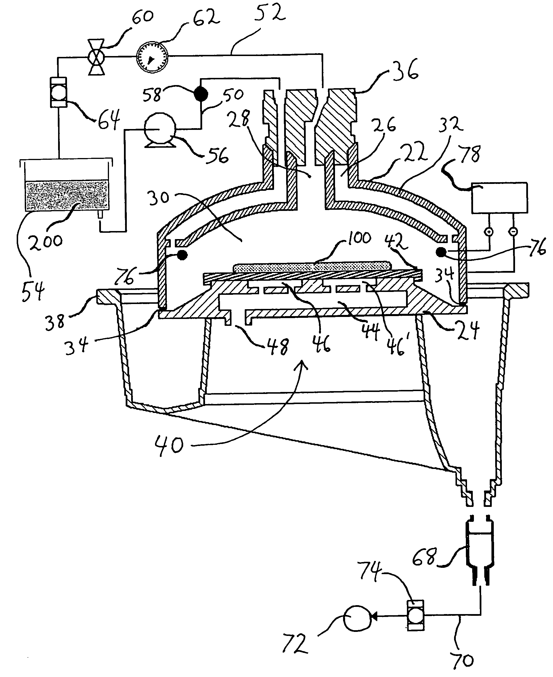
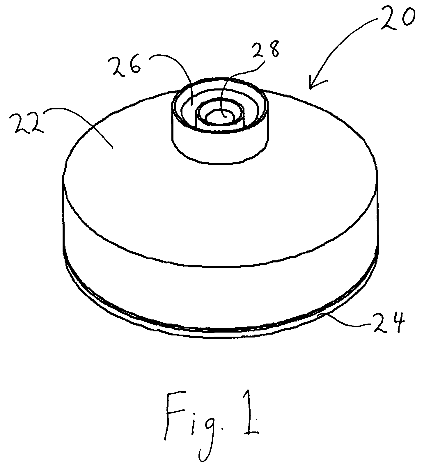
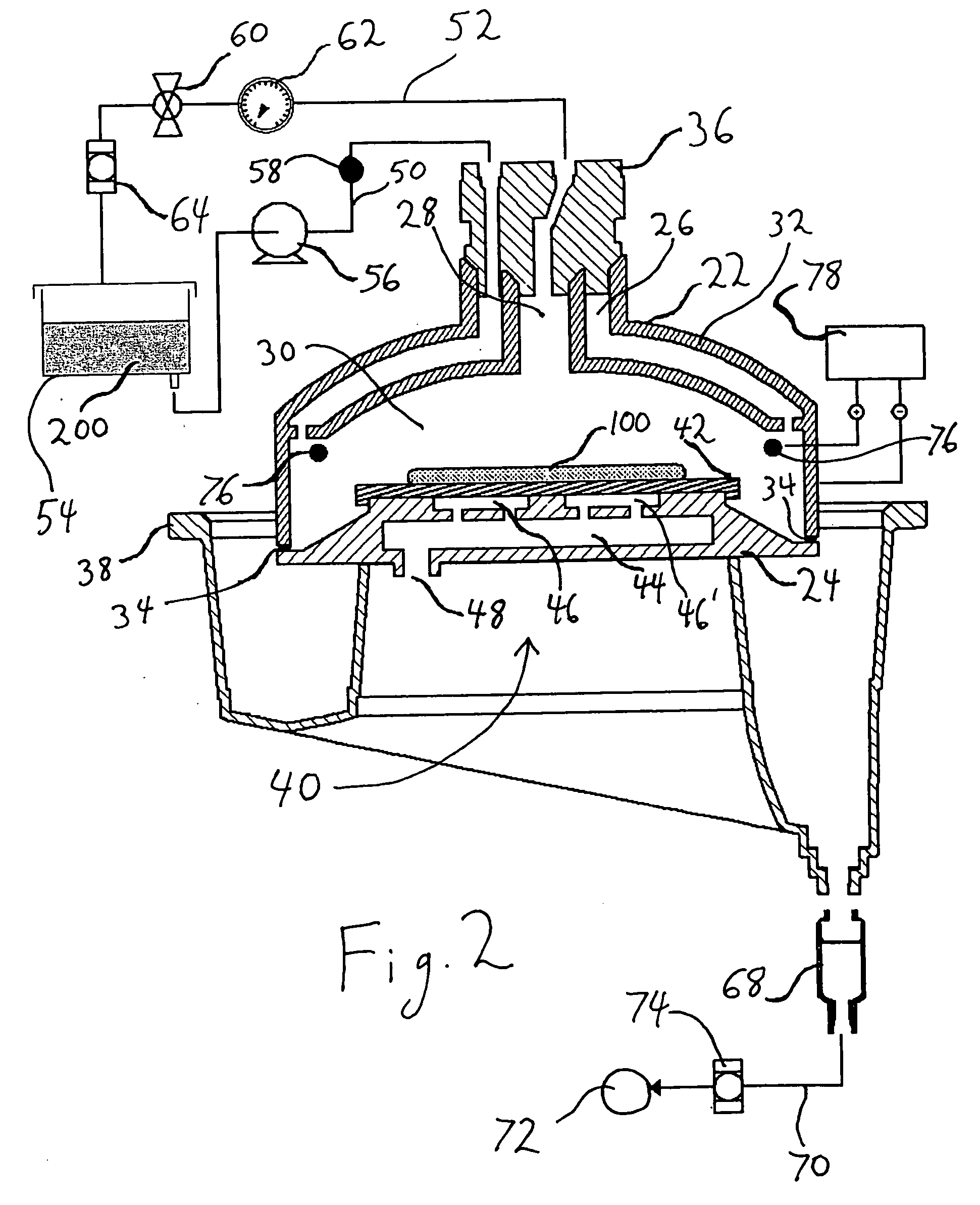
[0071] The preferred embodiment of the present invention comprises a metal plating (i.e., metal deposition) apparatus and method. The apparatus comprises a vessel or other enclosure to contain a substrate to be plated while the substrate is subjected to one or more plating processes and / or materials and fluids. Such processes include the electrolytic and electroless (i.e., autocatalytic) deposition of metal(s). As used herein, “substrate” is defined as any object comprising a surface onto which metal deposition is to occur, including, but not limited to, a semiconductor wafer. The present invention provides for the plating of a substrate in a single vessel without the need to transfer the substrate to other vessels for exposure to other plating fluids or process steps. As used herein, a “plating fluid” is any fluid to which a substrate is exposed during a plating process including, but not limited to, chemical solutions, rinsing solutions, and metal solutions. In the preferred embod...


PUM

PropertyMeasurementUnit
Temperatureaaaaaaaaaa
Volumeaaaaaaaaaa
Volumeaaaaaaaaaa

Abstract

The present invention comprises a metal plating apparatus and method, particularly suitable for autocatalytic (i.e., electroless) plating, comprising a pressurized sealable vessel for disposing a substrate to be plated and for the circulation of plating solutions wherein temperatures and pressure are highly controllable.

Description

CROSS-REFERENCE TO RELATED APPLICATIONS [0001] This application claims the benefit of the filing of U.S. Provisional Patent Application Ser. No. 60 / 541,687, entitled “Pressurized Autocatalytic Vessel and Vacuum Chuck”, filed Feb. 4, 2004. This application is also related to U.S. patent application Ser. No. 10 / 778,647, entitled “Apparatus and Method for Highly Controlled Electrodeposition”, filed Feb. 12, 2004, which claims priority of U.S. Provisional Patent Application Ser. No. 60 / 447,175, entitled “Electrochemical Devices and Processes”, filed Feb.12, 2003, and which is a continuation-in-part application of U.S. patent application Ser. No. 10 / 728,636, entitled “Coated and Magnetic Particles and Applications Thereof”, filed Dec.5, 2003, which claims priority of U.S. Provisional Patent Application Ser. No. 60 / 431,315, entitled “Solid Core Solder Particles for Printable Solder Paste”, filed on Dec. 5, 2002, and the specifications and claims thereof are incorporated herein by referenc...

Claims


Application Information

Patent Timeline
IPC IPC(8): C23C18/16C25D5/00C25D7/12C25D17/00C25D21/00
CPCC23C18/1619C25D5/003C25D17/001C25D7/123
Inventor BLECK, MARTINBERNER, ROBERT WAYNEMINOGUE, GERARDSANCHEZ, FERNANDO M.HANNON, MATHEWGRIEGO, THOMAS P.
Owner SURFECT TECH
Why Eureka
Try Eureka