CMOS device and method of manufacture

a technology of metal oxide semiconductor and manufacturing method, which is applied in the direction of semiconductor devices, semiconductor device details, electrical apparatus, etc., can solve the problems of reducing the performance of p-type transistors, reducing reducing the mobility of holes, so as to improve the performance of cmos devices, reduce stress and surface tension, and create surface tension

Active Publication Date: 2005-10-20
TAIWAN SEMICON MFG CO LTD
View PDF6 Cites 36 Cited by
  • Summary
  • Abstract
  • Description
  • Claims
  • Application Information

AI Technical Summary

Benefits of technology

[0012] Advantages of embodiments of the present invention include providing a nitride etch stop layer over an NMOS device and a bilayer etch stop including an oxide layer and a nitride layer over a PMOS device, which enhances CMOS device performance by creating surface tension to the channels of the NMOS and P

Problems solved by technology

However, in some applications, it may be undesirable to place a nitride layer or film directly over an underlying material layer.
For example, depositing a tensile nitride m

Method used


Image

  • CMOS device and method of manufacture
  • CMOS device and method of manufacture
  • CMOS device and method of manufacture

Examples


Embodiment Construction

[0017] The making and using of the presently preferred embodiments are discussed in detail below. It should be appreciated, however, that the present invention provides many applicable inventive concepts that can be embodied in a wide variety of specific contexts. The specific embodiments discussed are merely illustrative of specific ways to make and use the invention, and do not limit the scope of the invention.

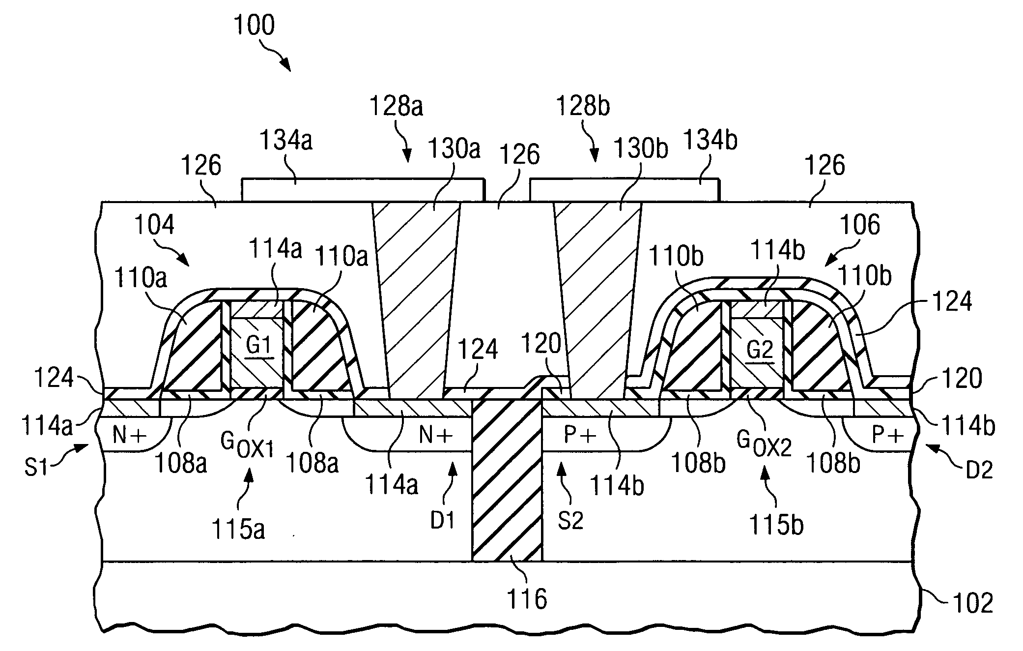
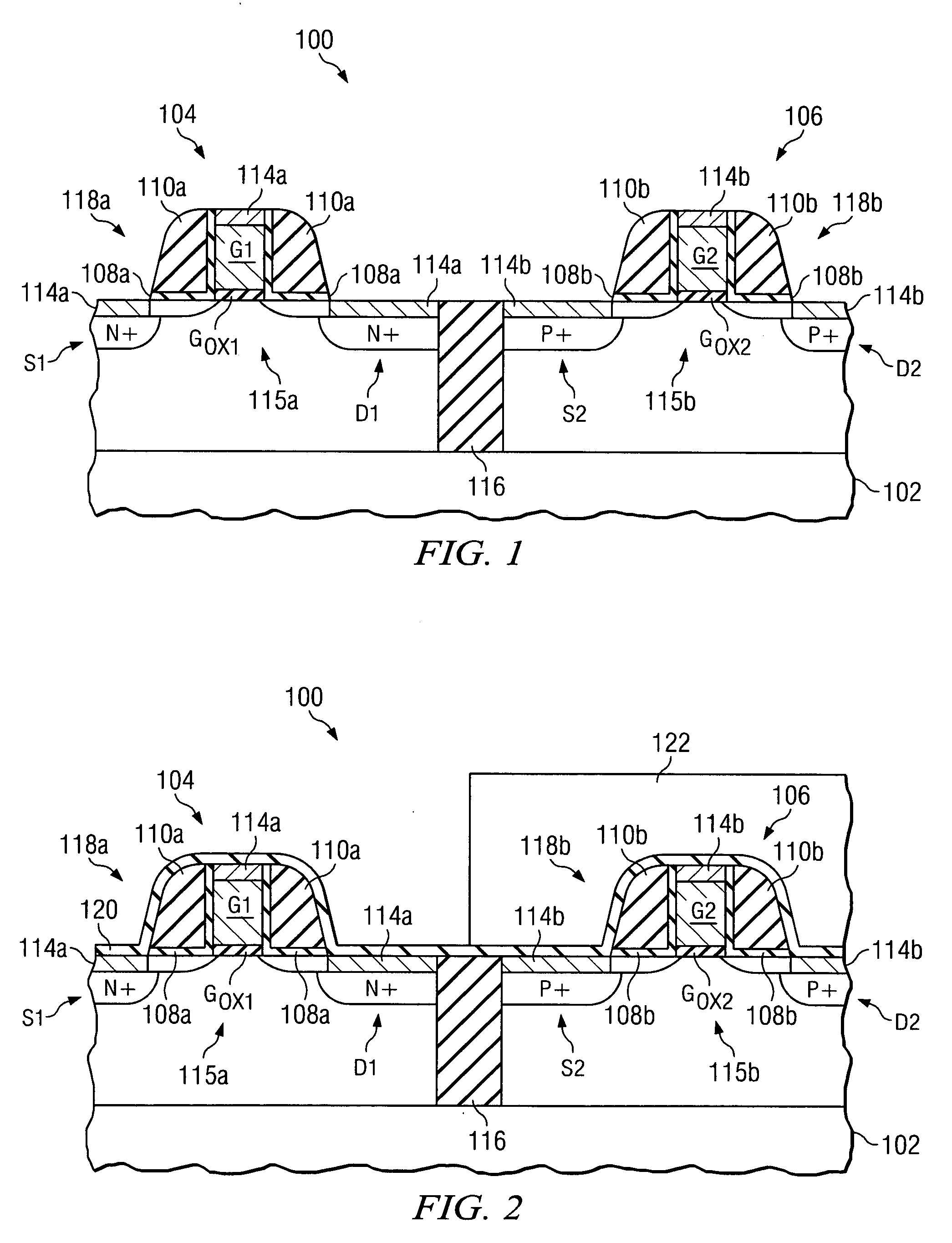
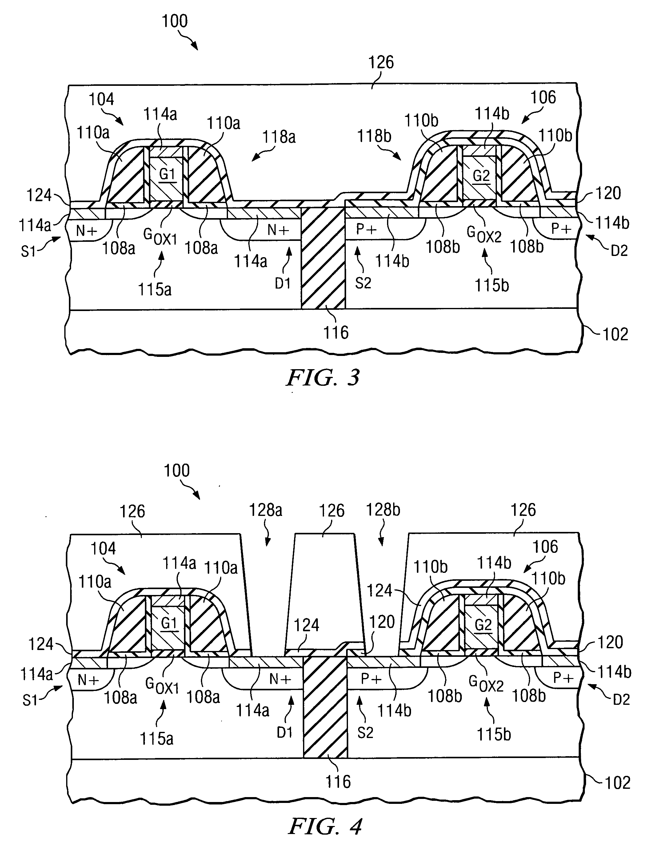
[0018] The present invention will be described with respect to preferred embodiments in a specific context, namely a CMOS device. Embodiments of the invention may also be applied, however, to other semiconductor device applications where it may be undesirable to deposit a nitride film or layer as an etch stop material directly over an underlying material layer. Note that in the drawings shown, only one PMOS device and one NMOS device are shown; however, there may be many PMOS and NMOS devices formed during each of the manufacturing processes described herein.

[0019]FIGS. 1 ...


PUM


Abstract

A CMOS device and manufacturing method thereof wherein a bilayer etch stop is used over a PMOS transistor, and a single etch stop layer is used for an NMOS transistor, for forming contacts to the source or drain of the CMOS device. A surface tension-reducing layer is disposed between the source or drain region of the PMOS transistor and an overlying surface tension-inducing layer. The surface tension-inducing layer may comprise a nitride material or carbon-containing material, and the surface tension-reducing layer may comprise an oxide material. Degradation of hole mobility in the PMOS transistor is prevented by the use of the surface tension-reducing layer of the bilayer etch stop.

Description

TECHNICAL FIELD [0001] The present invention relates generally to the manufacturing of semiconductor devices, and more particularly to a structure for and a method of manufacturing a complimentary metal oxide semiconductor (CMOS) device. BACKGROUND [0002] Semiconductor devices are used in a variety of electronic applications, such as personal computers, cell phones, digital cameras, and other electronic equipment, as examples. Semiconductor devices are typically fabricated by sequentially depositing insulating (or dielectric) layers, conductive layers and semiconductive layers of material over a semiconductor substrate, and patterning the various layers using lithography to form circuit components and elements thereon. [0003] A transistor is an element that is utilized extensively in semiconductor devices. There may be millions of transistors on a single integrated circuit (IC), for example. A common type of transistor used in semiconductor device fabrication is a metal oxide semico...

Claims


Application Information

Patent Timeline
IPC IPC(8): H01L21/8238H01L27/01
CPCH01L21/823807H01L29/7843H01L29/7842H01L21/823828
Inventor CHANG, SUN-JAYCHENG, CHIEN-LI
Owner TAIWAN SEMICON MFG CO LTD
Why Eureka
Try Eureka