Magnetic sensor having vertical hall device and method for manufacturing the same

Inactive Publication Date: 2005-10-20
DENSO CORP
View PDF9 Cites 120 Cited by
  • Summary
  • Abstract
  • Description
  • Claims
  • Application Information

AI Technical Summary

Benefits of technology

[0013] The above method provides the vertical Hall device having the substrate. The design degree of freedom

Problems solved by technology

However, it is difficult for the lateral Hall device to detect a magnetic field component parallel to t

Method used


Image

  • Magnetic sensor having vertical hall device and method for manufacturing the same
  • Magnetic sensor having vertical hall device and method for manufacturing the same
  • Magnetic sensor having vertical hall device and method for manufacturing the same

Examples


first embodiment

[0064] (First Embodiment)

[0065] The inventor have preliminarily studied about a Hall cell as a comparison of a Hall device according to a first embodiment of the present invention. Firstly, FIG. 46 explains a magnetic field detection principle of the Hall cell. Here, the Hall cell is capable of detecting not only a magnetic field but also an angle without contacting the cell. Therefore, for example, the Hall cell is mounted on a Hall IC so that the Hall cell detects an angle of, for example, a throttle valve opening degree in an auto motive vehicle.

[0066] In FIG. 46, when a current flows through a substance, and a magnetic field perpendicular to the current is applied to the substance, a new electric field is generated to be perpendicular to both of the current and the magnetic field. Thus, Hall voltage corresponding to the electric field is generated by this Hall effect. For example, in a Hall cell 100 in FIG. 46, a Hall plate as a magnetic field detection portion of the cell has ...

second embodiment

[0157] (Second Embodiment)

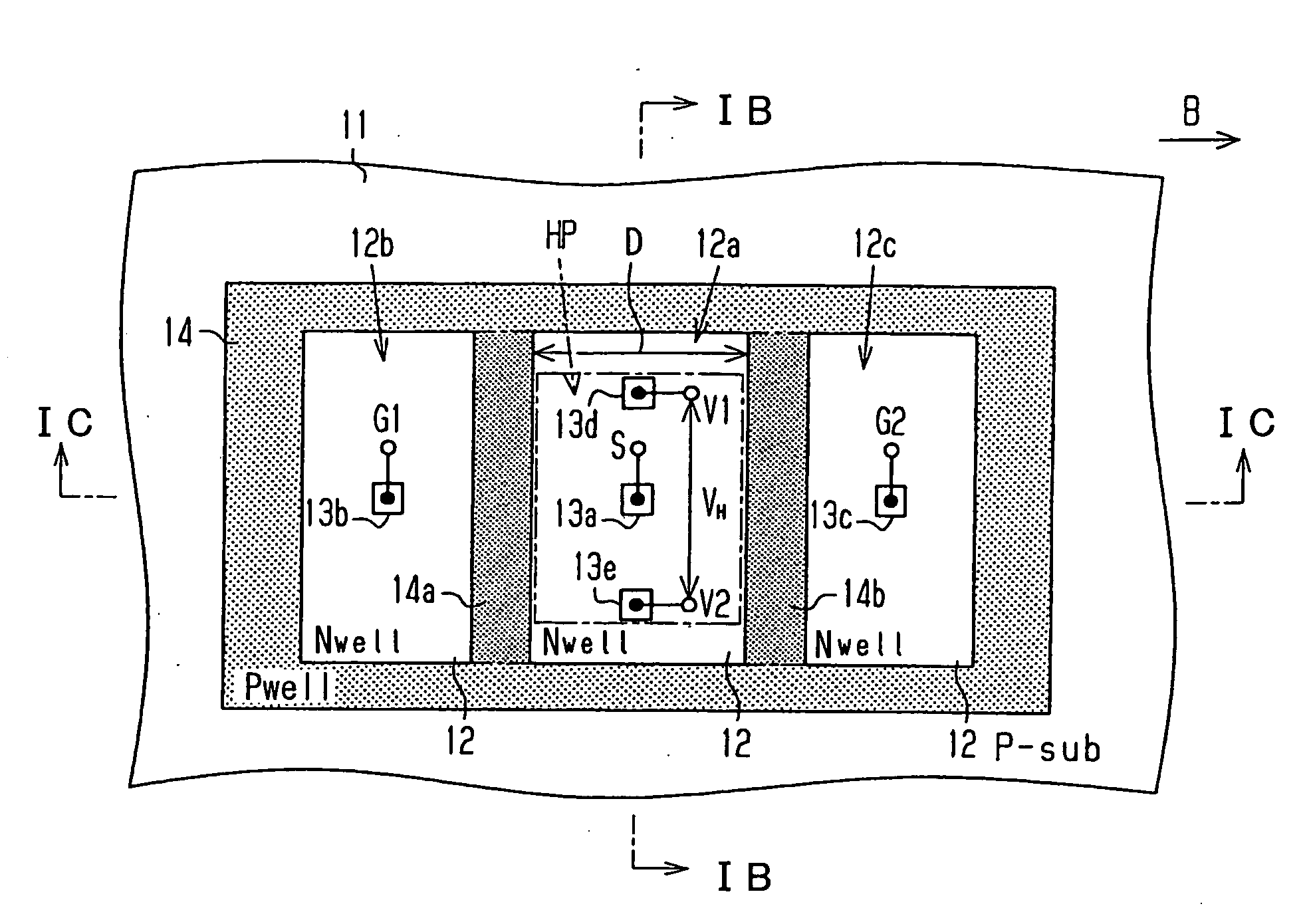
[0158] A vertical Hall device having a Hall cell portion 10 and a periphery circuit portion C10 according to a second embodiment of the present invention is shown in FIG. 16. The Hall device includes a field oxide film HL2 having a LOCOS construction. The field oxide film HL2 covers whole surface of the semiconductor region 12. Specifically, the field oxide film HL2 covers whole surface of the Hall cell portion 10 except for the contact regions 13a-13e for connecting to the wirings 16a-16c. The field oxide film HL2 protects the Hall cell portion 10 from damage caused in an ion implantation process, a plasma process or the like. Specifically, after the Hall cell portion 10 is formed in the Hall device, the ion implantation process or the plasma process is performed to form the periphery circuit portion C10. In this case, the field oxide film HL2 protects the Hall cell portion 10. Therefore, the field oxide film HL2 is used for manufacturing the Hall device t...

third embodiment

[0159] (Third Embodiment)

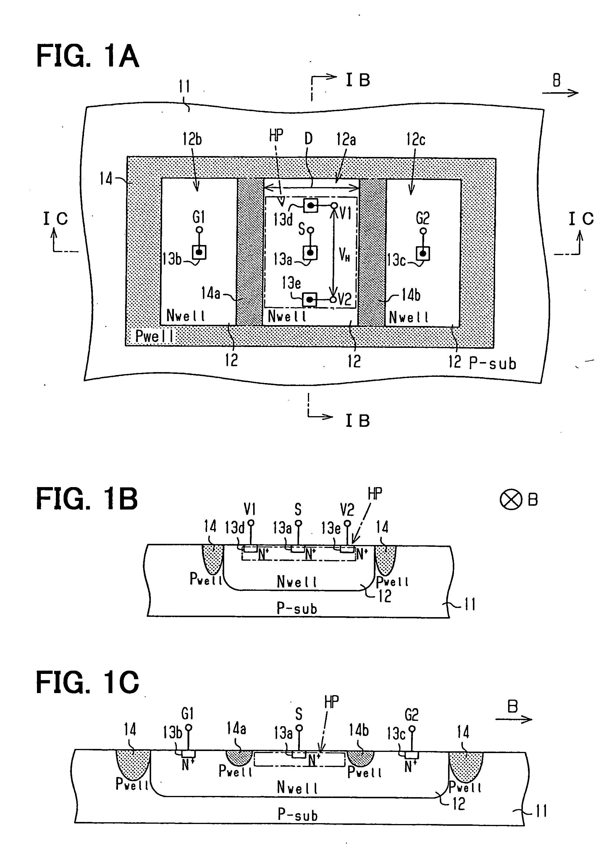
[0160] A vertical Hall device according to a third embodiment of the present invention is shown in FIGS. 17A to 17C. The Hall device has no diffusion layer 14, which separates the Hall device from other parts, as shown in FIG. 17A. Thus, the construction of the Hall device is simplified. Further, the dimensions of the Hall device are reduced. In this case, the semiconductor substrate 11 works as a separation wall instead of the diffusion region 14. The semiconductor substrate 11 surrounds the Hall device, i.e., the semiconductor region 12.

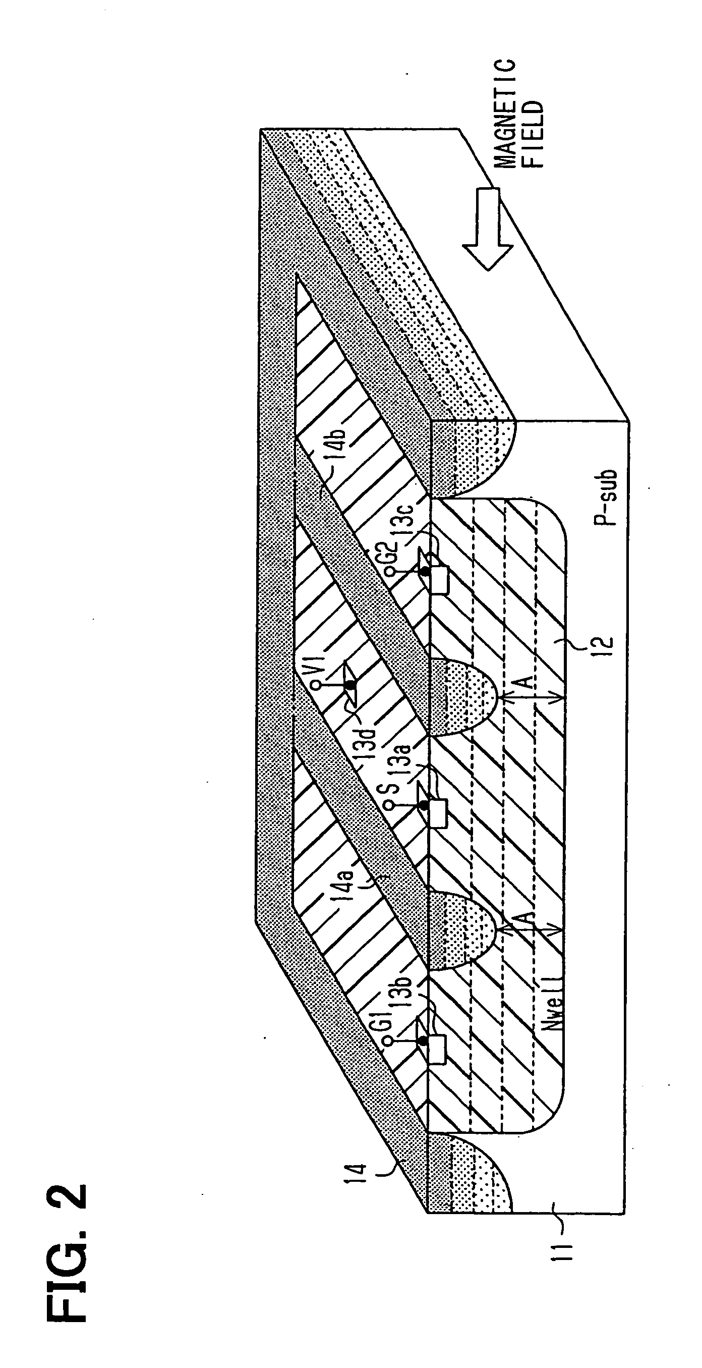
[0161]FIG. 18 shows the impurity concentration in the Hall device. Specifically, the impurity concentrations of the semiconductor region 12 and the diffusion layers 14a, 14b are shown. The impurity concentration of the diffusion layers 14a, 14b has the maximum concentration near the chip surface. Further, the impurity concentration of the semiconductor region 12 also has the maximum concentration near the chip surface.

[01...


PUM


Abstract

A vertical Hall device includes: a substrate; a semiconductor region having a first conductive type and disposed in the substrate; and a magnetic field detection portion disposed in the semiconductor region. The magnetic field detection portion is capable of detecting a magnetic field parallel to a surface of the substrate in a case where a current flows through the magnetic field detection portion in a vertical direction of the substrate. The semiconductor region is a diffusion layer including a conductive impurity doped and diffused therein. The semiconductor region is made of diffusion layer so that the device has high design degree of freedom.

Description

CROSS REFERENCE TO RELATED APPLICATIONS [0001] This application is based on Japanese Patent Applications No. 2004-100841 filed on Mar. 30, 2004, No. 2004-124460 filed on Apr. 20, 2004, and No. 2005-5653 filed on Jan. 12, 2005, the disclosures of which are incorporated herein by references. FIELD OF THE INVENTION [0002] The present invention relates to a magnetic sensor having a vertical Hall device and a method for manufacturing the same. BACKGROUND OF THE INVENTION [0003] In general, a lateral Hall cell detects a magnetic field component perpendicular to a substrate surface (i.e., a chip surface). The lateral Hall cell is disclosed in, for example, “Integrated three-dimensional magnetic sensor” in Journal of Institute of Electrical Engineers of Japan, Vol. 109-C, No. 7, pages 483-490 (1989). However, it is difficult for the lateral Hall device to detect a magnetic field component parallel to the substrate surface. [0004] To detect the magnetic field component parallel to the substr...

Claims


Application Information

Patent Timeline
IPC IPC(8): G01R33/02H01L21/00G01R33/07H01L21/8238H01L27/092H01L27/22H01L43/00H01L43/06H01L43/14
CPCG01R33/07G01R33/077G01R33/066H01L43/14H01L43/065H10N52/01H10N52/101
Inventor OOHIRA, SATOSHI
Owner DENSO CORP
Why Eureka
Try Eureka