GaN-based light-emitting diode structure

a technology of light-emitting diodes and gan-based diodes, which is applied in the direction of basic electric elements, electrical equipment, semiconductor devices, etc., can solve the problems of difficult to form excellent ohmic contact with indium tin oxide, and the inability to lower the working voltage of light-emitting diodes

Inactive Publication Date: 2005-10-27
SUPERNOVA OPTOELECTRONICS
View PDF4 Cites 53 Cited by
  • Summary
  • Abstract
  • Description
  • Claims
  • Application Information

AI Technical Summary

Benefits of technology

[0009] The invention provides a GaN-based light-emitting diode structure having an improved ohmic contact layer, and the purpose of the invention is to form a transparent conductive oxide layer on a GaN contact layer having a surface textured layer and to provide a textured layer to act as an ohmic contact layer with the transparent conductive oxide layer. The light-emitting diode structure includes: a substrate; a semiconductor stacked layer structure disposed on the substrate and having an

Problems solved by technology

However, in the diode structure, when the underlying p-type contact layer has a flat Ga-polarization surface, it is difficult to form an excellent ohmic contact with t

Method used


Image

  • GaN-based light-emitting diode structure
  • GaN-based light-emitting diode structure
  • GaN-based light-emitting diode structure

Examples


Embodiment Construction

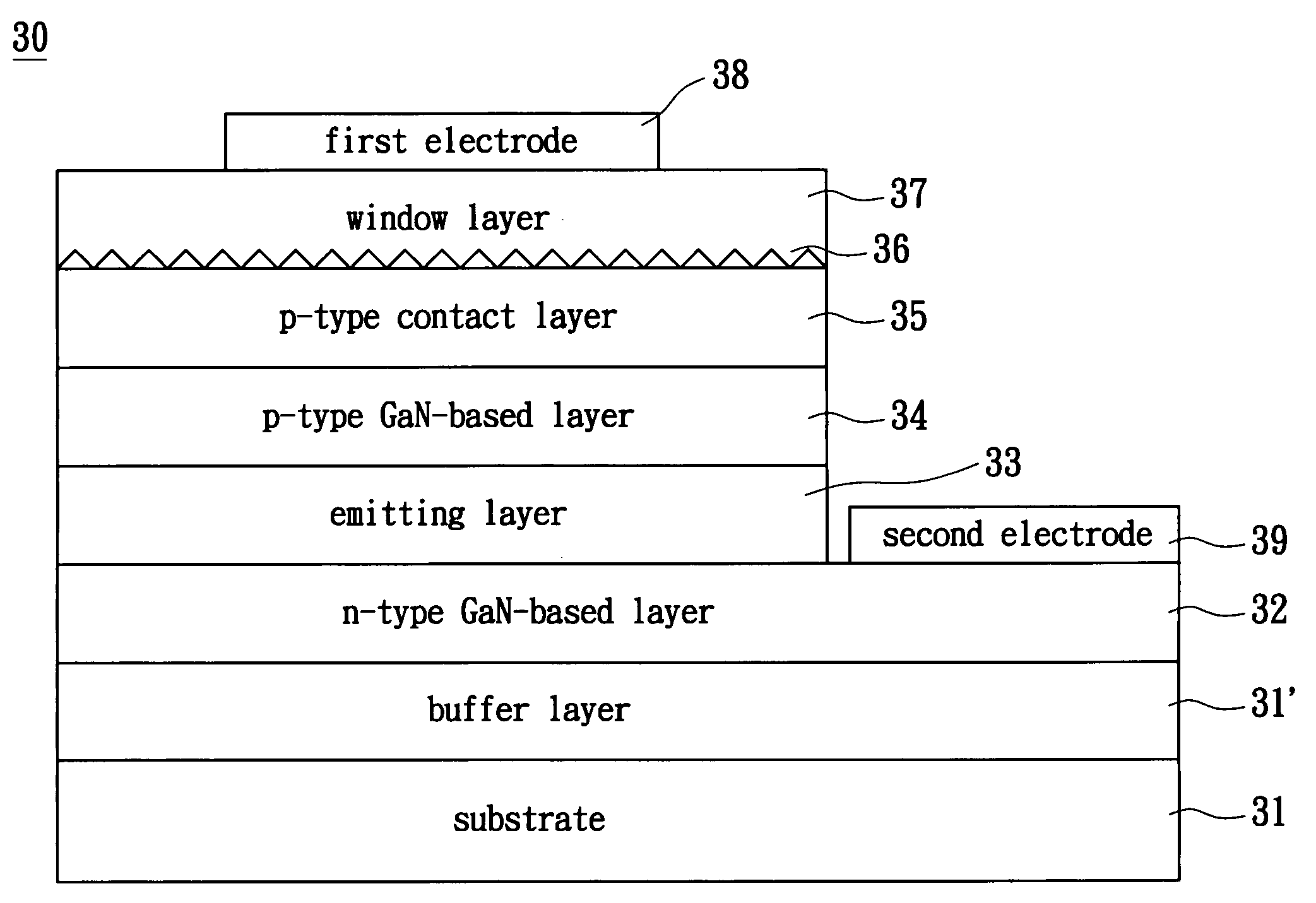
[0016] With reference to FIG. 3, a preferred example of a GaN-based light-emitting diode structure according to the present invention will be explained. As shown, according to the invention, the structure of a GaN-based light-emitting diode 30 includes a substrate 31, an n-type GaN-based layer 32, an emitting layer 33, a p-type GaN-based layer 34, a p-type contact layer 35, a textured layer 36, a window layer 37, a first electrode 38 and a second electrode 39. In the structure, a buffer layer 31′ may be additionally disposed on the substrate 31.

[0017] As described above, a semiconductor stacked layer structure formed on the substrate 31 comprises the n-type GaN-based layer 32, the emitting layer 33 and the p-type GaN-based layer 34 arranged sequentially from bottom to top. Further, the textured layer 36 is formed on the p-type GaN-based layer 34 and the p-type contact layer 35, and, as the window layer 37, a transparent conductive oxide layer is disposed on the textured layer 36, f...


PUM


Abstract

In a GaN-based light-emitting diode structure, a transparent conductive oxide layer is formed as a window layer on a GaN contact layer having a surface textured layer, and the textured layer acts as an ohmic contact layer with the transparent conductive oxide layer. Therefore, it is possible to reduce effectively the contact resistance and the working voltage, while the optical guiding effect is interrupted by the textured layer, to obtain thereby an enhancement of light extraction efficiency and thus an increase in the external quantum yield.

Description

BACKGROUND OF THE INVENTION [0001] 1. Field of the Invention [0002] The present invention relates to a GaN-based light-emitting diode structure, and particularly, to a GaN-based light-emitting diode structure having an improved ohmic contact layer. [0003] 2. Description of the Related Art [0004] Referring to FIG. 1, a conventional gallium nitride-based light-emitting diode structure 10 is shown to comprise a substrate 11, a GaN buffer layer 12, an n-type GaN layer 13, an InGaN emitting layer 14, a p-type GaN layer 15, a p-type GaN contact layer 16 and a transparent conductive layer 17. The layers 12 to 16 are herein referred to as an “epitaxial structure”. Further, a p-type metal electrode 18 is disposed on the transparent conductive layer 17 and an n-type metal electrode 19 is disposed on the n-type GaN layer 13. [0005] Conventionally, a p-type gallium nitride ohmic contact layer 16 has a poor conductivity; in other words, the current tends to be confined to a region beneath the p-...

Claims


Application Information

Patent Timeline
IPC IPC(8): H01L33/02H01L33/22H01L33/32H01L33/42
CPCH01L33/02H01L33/42H01L33/32H01L33/22
Inventor HON, SCHANG-JINGLAI, MU-JENCHAN, CHI-FENGHUANG, JENN-BINCHIANG, CHEN-FU
Owner SUPERNOVA OPTOELECTRONICS
Why Eureka
Try Eureka