
Method for forming organic thin film

Inactive Publication Date: 2005-10-27
SONY CORP
View PDF17 Cites 6 Cited by
  • Summary
  • Abstract
  • Description
  • Claims
  • Application Information

AI Technical Summary

Benefits of technology

[0010] The above-mentioned method for forming an organic thin film has the advantage that the film deposited on the surface of the substrate is composed solely of the film-forming component of organic material which has been transported and fed into the reaction chamber. Film forming in this manner eliminates inhomogeneous mixing of film-forming components or reaction heat due to reactions between film-forming components.

Problems solved by technology

Unfortunately, the rate of evaporation does not change linearly with temperature.
The rate of evaporation even becomes unstable as the temperature changes, and this makes accurate control difficult.
Moreover, the rate of evaporation does not respond quickly to the change of temperature, and this results in a long processing time and poor productivity.
Unfortunately, the forming of organic thin film by the OVPD method has the following disadvantage.
Therefore, the organic precursor substances do not mix homogeneously in the reactor or there is an uneven temperature distribution in the reactor even in the case of homogeneous mixing.
This makes the chemical reaction irregular, which in turn leads to variation in quality of the organic thin film formed on the surface of the substrate.
Therefore, the OVPD method applied to the production of organic EL elements having organic layers (including an emitting layer) formed by laminating a plurality of organic thin films as mentioned above has the disadvantage that the previously formed organic layer is deteriorated by reaction heat which is evolved when another organic layer is formed later.
This leads to elements with inadequate characteristics.

Method used


Image

  • Method for forming organic thin film
  • Method for forming organic thin film
  • Method for forming organic thin film

Examples


Embodiment Construction

[0016] The invention will be described in more detail with reference to the accompanying drawings.

[Film-forming Apparatus]

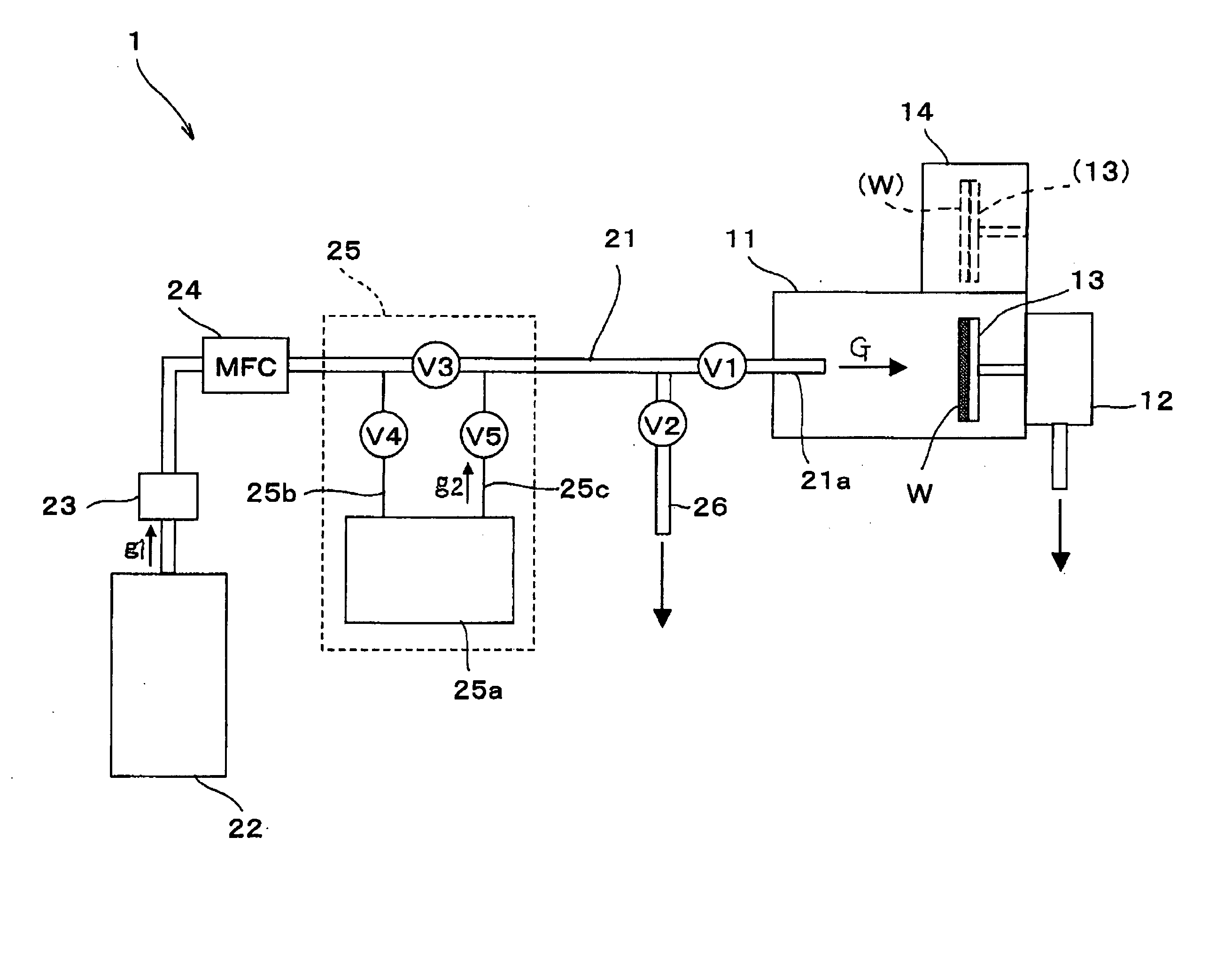
[0017]FIG. 1 schematically shows an example of the film-forming apparatus to form organic thin films according to the embodiment of the present invention. The film-forming apparatus 1 is equipped with a reaction chamber 11 to accommodate a substrate W on which organic thin films are to be formed.

[0018] The reaction chamber 11 is equipped with an exhaust system 12, which keeps the reaction chamber 11 at a prescribed pressure. The exhaust system 12 is so constructed as to pass the exhaust gas through a trap (not shown) that catches residual materials and discharges only inert gas, such as nitrogen (explained later), through a scrubber.

[0019] The reaction chamber 11 is provided with a substrate support 13 to hold a substrate W. It is also provided with a temperature controlling mechanism that keeps the supported substrate W at a prescribed temperature. It is als...


PUM

PropertyMeasurementUnit
Compositionaaaaaaaaaa

Abstract

A method for forming, without heat evolution, an organic thin film with homogeneous quality on the surface of the substrate. The method consists of vaporizing a single film-forming component of organic material, thereby evolving a film-forming gas (g2), transporting and feeding the film-forming gas (g2) into a reaction chamber (11) in which a substrate (W) is placed, and depositing the organic material, while keeping the film-forming component, on the surface of the substrate (W) in the reaction chamber (11). The substrate (W) is kept cooled while the organic material is being deposited. The film-forming gas (g2) is transported and fed into the reaction chamber (11) by using a carrier gas, such as an inert gas (g1). The deposition of the organic material is repeated so that films differing in composition are formed one over another.

Description

TECHNICAL FIELD [0001] The present invention relates to a method for forming an organic thin film and, more particularly, to a method for forming an organic thin film which can be suitably applied to forming an organic thin film constituting an optical element such as organic EL element. BACKGROUND ART [0002] Electroluminescence (EL for short hereinafter) of an organic material is used for an organic EL element which is composed of an anode, a cathode, and an organic layer held between the two electrodes. The organic EL element of this structure emits different colors depending on the material selected for the organic layer. If a plurality of organic EL elements emitting different colors are arranged in a specific manner, it will be possible to construct a display unit capable of multi-color display or full-color display. [0003] Production of such organic EL elements as mentioned above involves vacuum deposition to form the organic layer. Vacuum deposition is one method of depositin...

Claims


Application Information

Patent Timeline
IPC IPC(8): H05B33/10C23C14/12C23C14/24H01L51/40H01L51/50H01L51/56
CPCC23C14/12C23C14/228H01L51/56H01L51/001C23C14/243H10K71/164H10K71/40H10K71/30H10K71/00
Inventor YANASHIMA, KATSUNORINARUI, HIRONOBUMEMEZAWA, AKIHIKOSASAKI, KOJI
Owner SONY CORP
Learn More