

Flash memory device with ATA/ATAPI/SCSI or proprietary programming interface on PCI express
a flash memory device and programming interface technology, applied in the direction of instruments, input/output to record carriers, computing, etc., can solve the problems of data storage technologies that are still confronted with several technical limitations and difficulties, speed of data transfer, inability to simultaneously read and write data, etc., and achieve the effect of convenient use for different host platforms
- Summary
- Abstract
- Description
- Claims
- Application Information
AI Technical Summary
Benefits of technology
Problems solved by technology
Method used
Image

Examples
Embodiment Construction
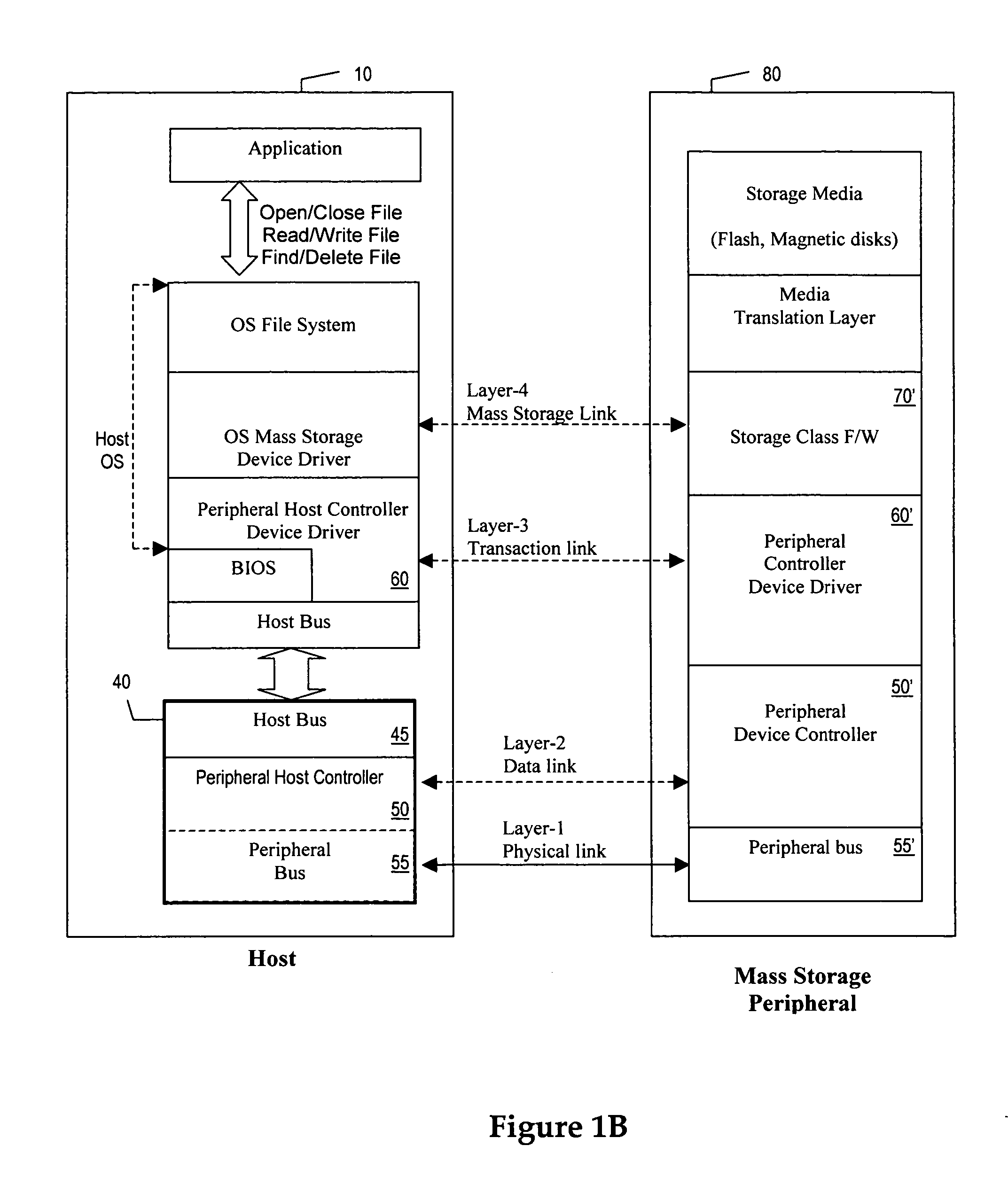
[0026] Referring to FIG. 2 for a functional block diagram for showing host computer 100 interfaces through a PCI Express link 108 to a memory device 120. The memory device can be an internal memory device as part of the host computer or as shown in FIG. 2, as an externally adaptable flash memory device 120. In a preferred embodiment, the memory device 120 includes a flash memory 125 controlled by a controller 130 that can be either an ATA / ATAP / SCSI host controller or a proprietary storage device controller. The host computer 100 is operated with an operation system (OS) 140 that controls the file system 150 and another host mass storage device driver 135′. The host mass storage device driver 135′ supports either an ATA / ATAP programming interface 160-1 or SCSI programming interface 160-2 or proprietary interface 160-3.
[0027] Base on the architecture as shown in FIG. 2, a READ operation of data from the flash memory 125 is processed by first retrieving data from the nonvolatile flash...
PUM
 Abstract
Description
Claims
Application Information