Bipolar transistor having self-aligned silicide and a self-aligned emitter contact border

a bipolar transistor and contact border technology, applied in the field of bipolar transistors, can solve the problem of high base resistance (rb) and achieve the effect of reducing the emitter resistan

Active Publication Date: 2005-11-03
IBM CORP
View PDF6 Cites 28 Cited by
  • Summary
  • Abstract
  • Description
  • Claims
  • Application Information

AI Technical Summary

Benefits of technology

[0007] A further object of the present invention is to provide a bipolar transistor wherein the parasitic resistance and capacitance have been substantially reduced.
[0009] A yet further object of the present invention is to provide a bipolar transistor in which the polysilicon component of the base resistance Rb(poly) is significantly reduced.
[0012] In addition, a block emitter region eliminates the emitter-to-base parasitic capacitance component across the isolation oxide Ceb (TEOS) as shown in FIG. 1. Moreover, in the present invention, the block emitter region can be silicided to further reduce the emitter resistance Re.
[0013] Another benefit of providing a bipolar transistor with a block emitter region is that the emitter contact border can be defined in a self-aligned manner with a spacer or double spacer. Furthermore, the self-aligned emitter contact border provided by the present invention has the same dimension as that for the contact defined by lithography in the prior art process (see FIG. 1).

Problems solved by technology

The limitation of extending the silicide closer to the emitter leads to high base resistance (Rb).

Method used


Image

  • Bipolar transistor having self-aligned silicide and a self-aligned emitter contact border
  • Bipolar transistor having self-aligned silicide and a self-aligned emitter contact border
  • Bipolar transistor having self-aligned silicide and a self-aligned emitter contact border

Examples


Embodiment Construction

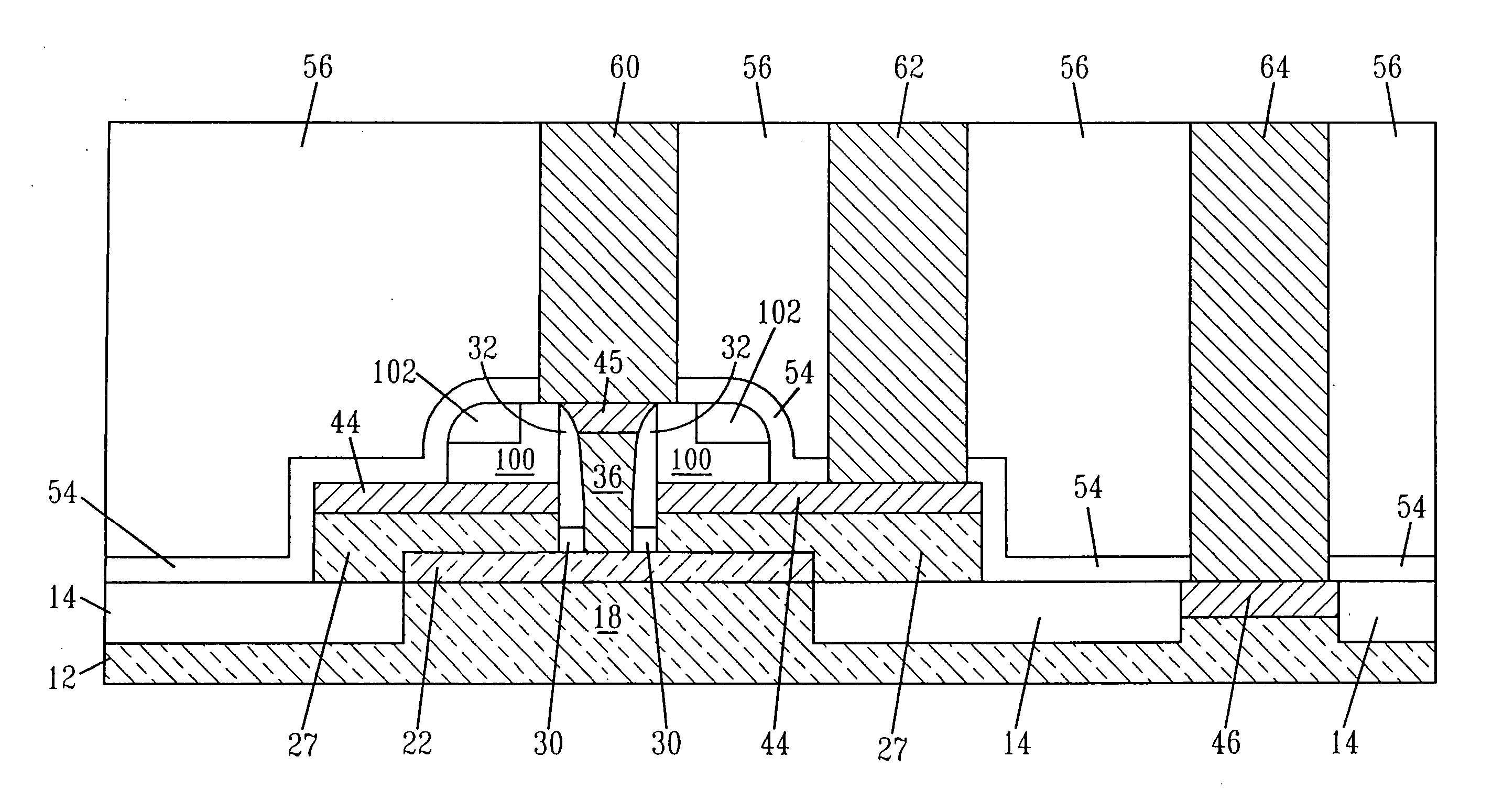
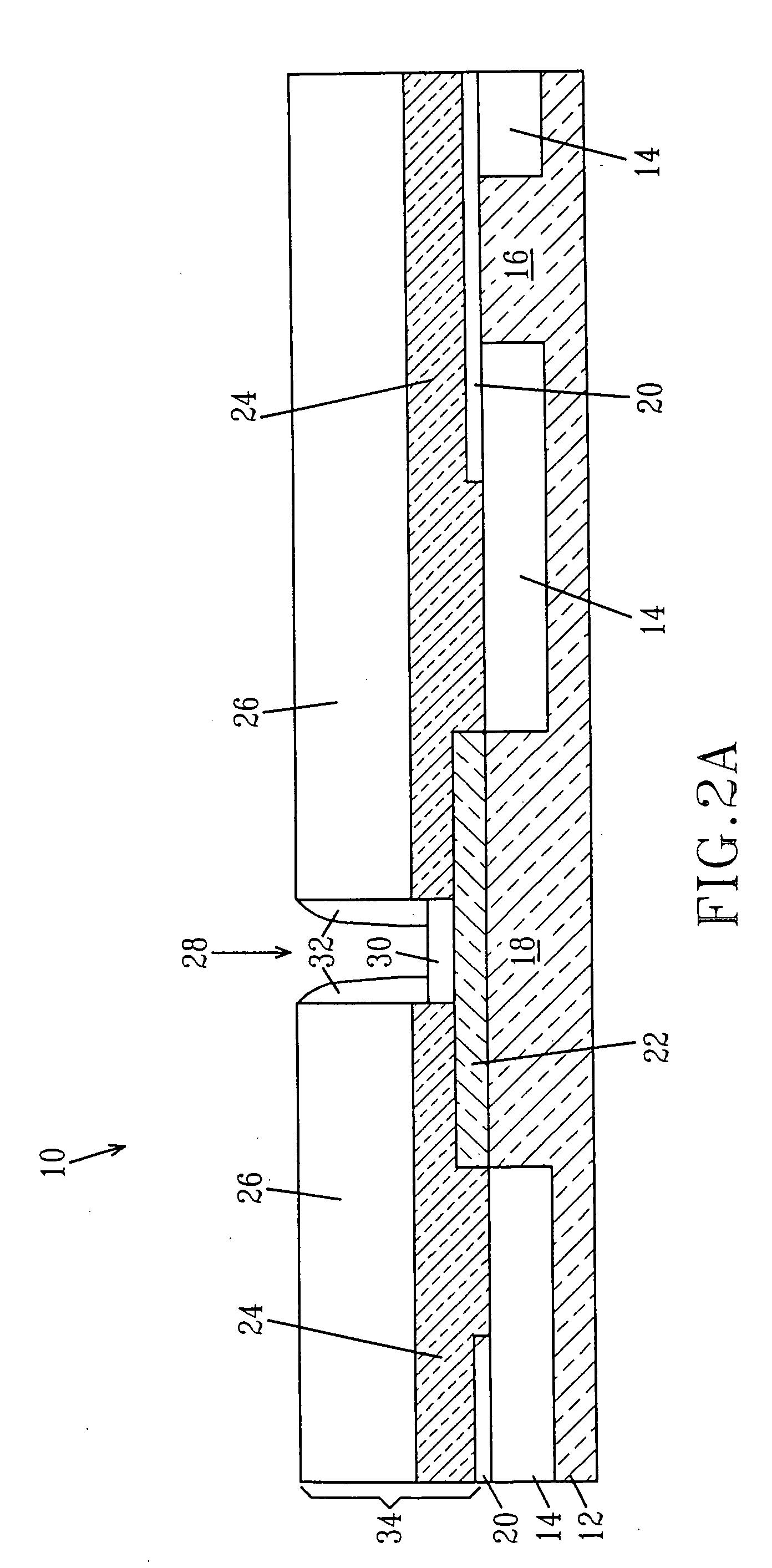
[0052] The present invention, which provides bipolar transistors having self-aligned silicides and self-aligned emitter contact border as well as methods of fabricating the same, will now be described in greater detail by referring to the drawings that accompany the present application. In the accompanying drawings, like and / or corresponding elements are referred to by like reference numerals.

[0053] The drawings of the present application illustrate only the heterojunction bipolar transistor (HBT) area. For clarity, the CMOS device areas as well as other areas of a typical BiCMOS structure are not shown in drawings. These other areas not shown lay to the periphery of the HBT area shown. Additionally, although a single HBT device area is shown, the present invention can be used in forming a plurality of HBTs on top of a single substrate.

[0054] Reference is first made to FIGS. 2A-2H which illustrate a first embodiment of the present invention. In this embodiment, a block polysilicon...


PUM


Abstract

The present invention provides a bipolar transistor having a raised extrinsic base silicide and an emitter contact border that are self-aligned. The bipolar transistor of the present invention exhibit reduced parasitics as compared with bipolar transistors that do not include a self-aligned silicide and a self-aligned emitter contact border. The present invention also is related to methods of fabricating the inventive bipolar transistor structure. In the methods of the present invention, a block emitter polysilicon region replaces a conventional T-shaped emitter polysilicon.

Description

FIELD OF THE INVENTION [0001] The present invention relates to bipolar transistors, and more particularly to a bipolar transistor having a raised extrinsic base with a silicide region and an emitter contact border that are self-aligned to the emitter. The bipolar transistor of the present invention exhibits reduced parasitics as compared with a bipolar transistor that does not include a self-aligned silicide and a self-aligned emitter contact border. The present invention also relates to various methods of fabricating a bipolar transistor structure having a raised extrinsic base with a silicide region and an emitter contact border that are self-aligned to the emitter. BACKGROUND OF THE INVENTION [0002] Cut-off frequency (fT) and maximum oscillation frequency (fmax) are the most representative measures of operation speed for high-speed transistors. Hence, the design and optimization efforts for high-speed transistors are mostly directed towards maximization of the aforementioned para...

Claims


Application Information

Patent Timeline
Patent Type & Authority Applications(United States)
IPC IPC(8): H01L21/28H01L21/331H01L21/8249H01L29/08H01L29/417H01L29/423H01L29/732H01L29/737
CPCH01L21/8249H01L29/0804H01L29/41708H01L29/42304H01L29/7378H01L29/66287H01L29/732H01L29/7375H01L29/66242
Inventor AHLGREN, DAVID C.FREEMAN, GREGORY G.KHATER, MARWAN H.VOLANT, RICHARD P.
Owner IBM CORP
Why Eureka
Try Eureka