
Low-k interlevel dielectric layer (ILD) and method

a dielectric layer and low-k technology, applied in the direction of chemical vapor deposition coating, basic electric elements, coatings, etc., can solve the problems of cvd film with a k value of 2.5, general incompatibility with chemical mechnical polishing, and physical property of beong soft can give rise to problems

Inactive Publication Date: 2005-11-03
IBM CORP
View PDF8 Cites 17 Cited by
  • Summary
  • Abstract
  • Description
  • Claims
  • Application Information

AI Technical Summary

Benefits of technology

[0023] It is therefore an aspect of the invention to provide an improved technique for forming an Interlevel Dielectric Layer (ILD), particularly a low-k ILD.
[0024] According to the invention, an interlevel dielectric layer (ILD) comprises a low-k dielectric layer; and a low-k dielectric film, deposited under compressive stress atop the dielectric layer. The dielectric layer comprises a low-k material, such as an organosilicon glass (OSG) or a SiCOH material. The dielectric film has a thickness of 2%-10% of the thickness of the dielectric layer, a similar chemical composition to the dielectric layer, but a different morphology than the dielectric layer. The dielectric film is deposited under compressive stress, in situ , at or near the end of the dielectric layer deposition by altering a process that was used to deposit the low-k dielectric layer.

Problems solved by technology

As a result, it is very difficult to prepare a CVD film with a k value of <2.5.
A problem with some low-k materials, particularly those that are organic in nature, is that they are generally not compatible with chemical mechnical polishing (CMP).
Because of their organic nature these materials are innately soft This physical property of beong soft can give rise to problems during semiconductor processing, particularly during planarization, by chemical mechanical polishing (CM P).
But one problem associated with them is that when in thin film form, they are found to be in a state of high tensile stress.

Method used


Image

  • Low-k interlevel dielectric layer (ILD) and method
  • Low-k interlevel dielectric layer (ILD) and method

Examples


Embodiment Construction

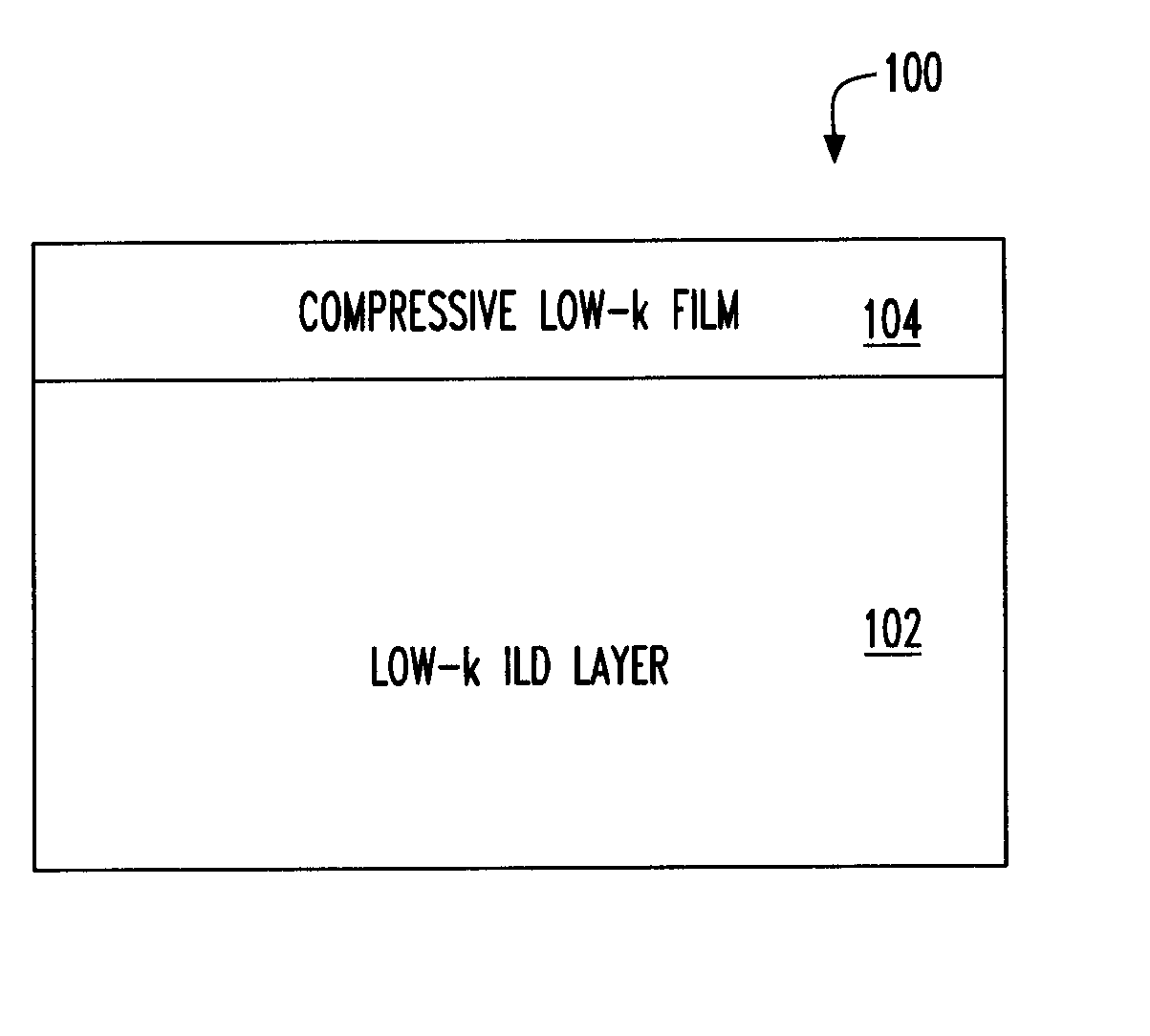
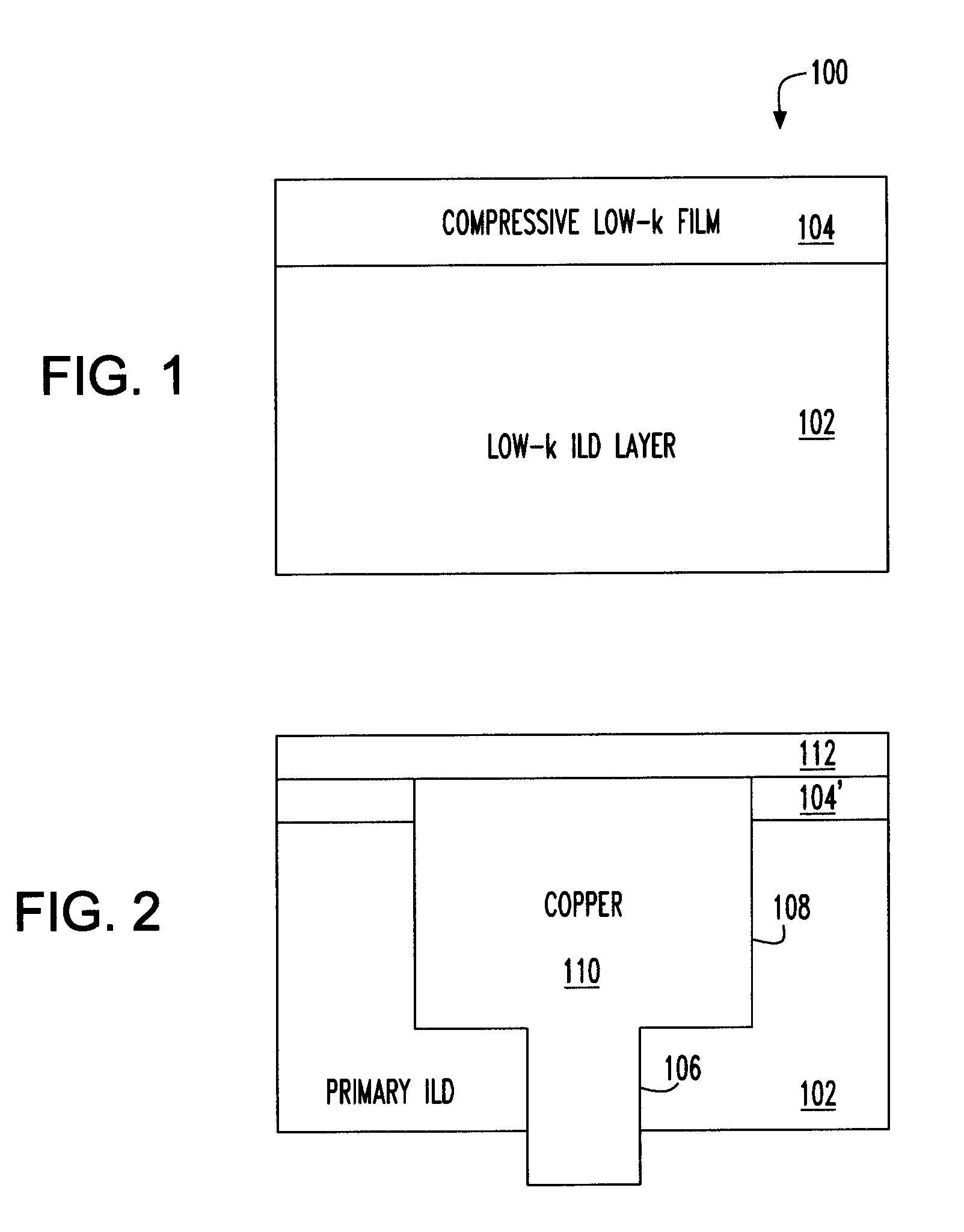
[0028] In the description that follows, numerous details are set forth in order to provide a thorough understanding of the present invention. It will be appreciated by those skilled in the art that variations of these specific details are possible while still achieving the results of the present invention. Well-known elements and processing steps are generally not described in detail in order to avoid unnecessarily obfuscating the description of the present invention.

[0029] Materials (e.g., silicon dioxide) may be referred to by their formal and / or common names, as well as by their chemical formula. Regarding chemical formulas, numbers may be presented in normal font rather than as subscripts. For example, silicon dioxide may be referred simply as “oxide” or by its chemical formula SiO2.

[0030] In the description that follows, exemplary dimensions may be presented for an illustrative embodiment of the invention. The dimensions should generally not be interpreted as limiting. They a...


PUM

PropertyMeasurementUnit
dielectric constantaaaaaaaaaa
dielectric constantsaaaaaaaaaa
poweraaaaaaaaaa

Abstract

An interlevel dielectric layer (ILD) comprises a low-k dielectric layer; and a low-k dielectric film, deposited under compressive stress, atop the dielectric layer. The dielectric layer comprises a low-k material, such as an organosilicon glass (OSG) or a SiCOH material. The dielectric film has a thickness, which is 2%-10% of the thickness of the dielectric layer, has a similar chemical composition to the dielectric layer, but has a different morphology than the dielectric layer. The dielectric film is deposited under compressive stress, in situ, at or near the end of the dielectric layer deposition by altering a process that was used to deposit the low-k dielectric layer.

Description

BACKGROUND OF INVENTION [0001] The invention relates to the fabrication of integrated circuit (IC) devices, particularly to dielectric materials, and more particularly to the fabrication of a low-k interlevel dielectric layer (ILD). [0002] Semiconductor devices are typically joined together to form useful circuits using interconnect structures comprising conductive materials (e.g., metal lines) such as copper (Cu) or aluminum (Al) and dielectric materials such as silicon dioxide (SiO2). The speed of these interconnects can be roughly assumed to be inversely proportional to the product of the line resistance (R), and the capacitance (C) between lines. To reduce the delay and increase the speed, it is desirable to reduce the capacitance (C). This can be done by reducing the dielectric constant k of the dielectric material in the interlevel dielectric layers (ILDs). Thus, there is considerable interest in developing low-k materials as well as deposition methods for them that are compat...

Claims


Application Information

Patent Timeline
Patent Type & Authority Applications(United States)
IPC IPC(8): H01L23/58
CPCC23C16/401H01L21/02126H01L21/022H01L21/02216H01L21/02274H01L23/53295H01L21/31633H01L21/76829H01L21/76835H01L23/5329H01L21/02362H01L2924/0002H01L21/02203H01L2924/00
Inventor ANGYAL, MATTHEWBARTH, EDWARD PAULDAS, SANJIT KUMARDAVIS, CHARLES ROBERTHICHRI, HABIBLANDERS, WILLIAM FRANCISLEE, JIA
Owner IBM CORP
Learn More