Solid-state imaging device, method of manufacturing solid-state imaging device and method of driving solid-state imaging device

a solid-state imaging and imaging device technology, applied in the direction of radioation control devices, television system scanning details, television systems, etc., can solve the problems of difficult to improve the efficiency of receiving light, and achieve the effect of sufficient dynamic range, sufficient sensitivity, and favorable characteristics

Inactive Publication Date: 2005-11-10
SONY SEMICON SOLUTIONS CORP
View PDF3 Cites 6 Cited by
  • Summary
  • Abstract
  • Description
  • Claims
  • Application Information

AI Technical Summary

Benefits of technology

[0035] Therefore, according to an embodiment of the present invention, a solid-state imaging device having favorable characteristics can be obtained in which a sufficient amount of electric charge can be received by light-receiving sensor portions, and sufficient sensitivity and sufficient dynamic range are secured.
[0036] Further, according to an embodiment of the present invention, problems (deterioration in sensitivity, a narrow dynamic range, and the like) conspicuously occurred when a solid-state imaging device is made minute can be solved, so that a solid-state imaging device can be made minute and the increase in the number of pixels and high density of a solid-state imaging device can be obtained. Furthermore, the miniaturization of a solid-state imaging device can also be achieved.

Problems solved by technology

Hence, it is difficult to improve the efficiency in receiving light.

Method used


Image

  • Solid-state imaging device, method of manufacturing solid-state imaging device and method of driving solid-state imaging device
  • Solid-state imaging device, method of manufacturing solid-state imaging device and method of driving solid-state imaging device
  • Solid-state imaging device, method of manufacturing solid-state imaging device and method of driving solid-state imaging device

Examples


Embodiment Construction

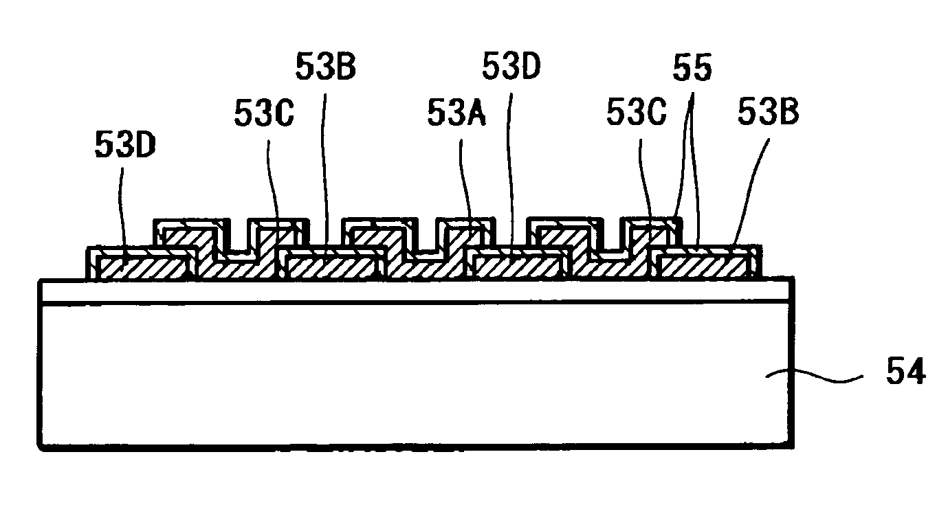
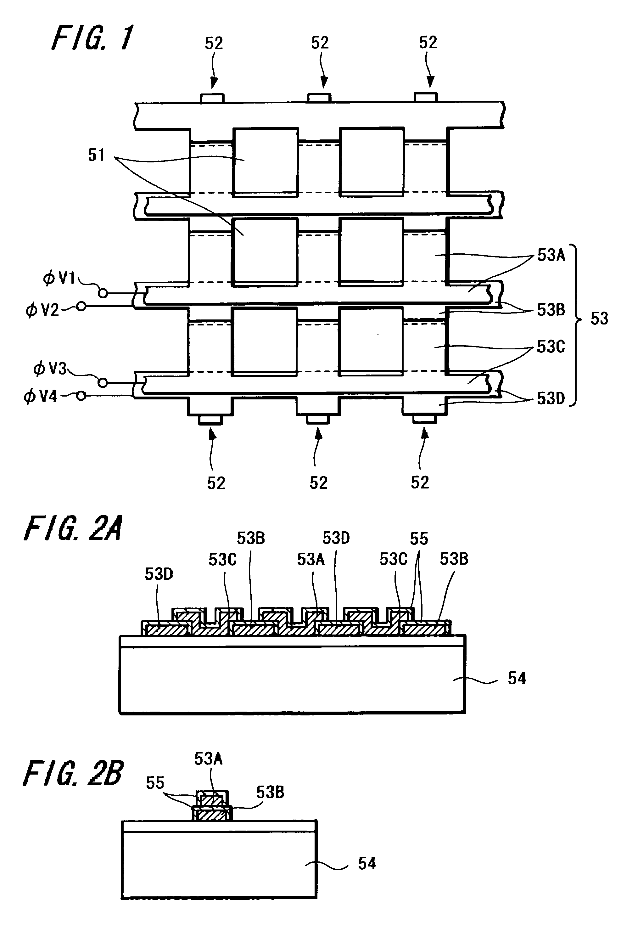
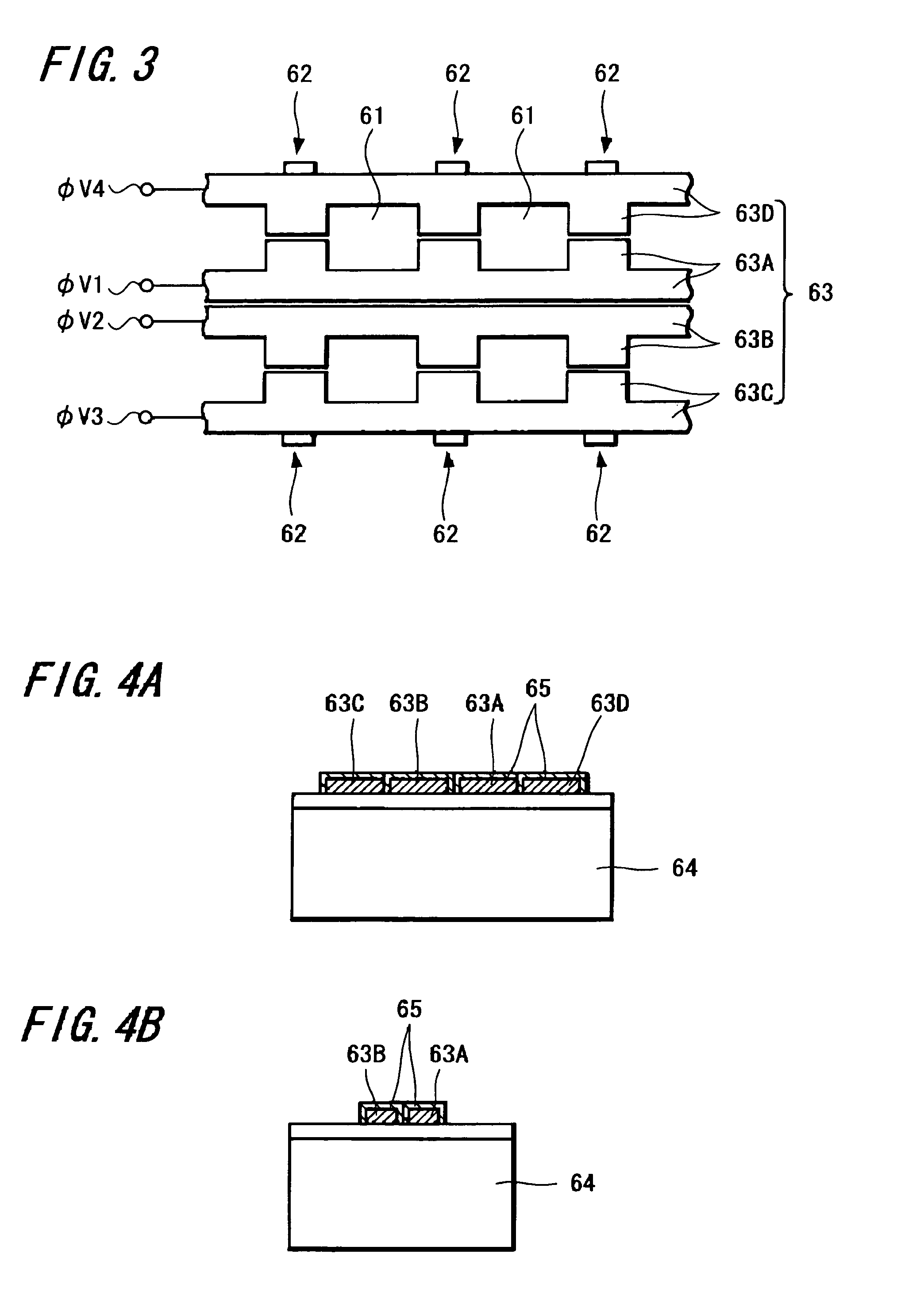
[0043]FIG. 5 is a schematic constitutional view (plan view) showing a solid-state imaging device according to an embodiment of the present invention.

[0044] This embodiment is a case in which the present invention is applied to a CCD solid-state imaging device.

[0045] In this solid-state imaging device, a vertical transfer resistor 2 is formed on one side of each column of light-receiving sensor portions 1 arranged in the form of a matrix to constitute an imaging area.

[0046] Each light-receiving sensor portion 1 constitutes a pixel, and in this embodiment, one portion is provided per pixel.

[0047] Outside the imaging area, although not shown in the figure, a horizontal transfer resistor is provided to be connected to one end of the vertical transfer resistor 2, and an output portion is provided at one end of the horizontal transfer resistor.

[0048] Further, FIG. 6A is a sectional view of the vertical transfer resistor 2 of the solid-state imaging device shown in FIG. 5; and FIG. 6B...


PUM


Abstract

A solid-state imaging device capable of securing sufficient sensitivity and obtaining favorable characteristics is provided. The solid-state imaging device includes a charge-transfer portion 2 provided on one side of each column of light-receiving sensor portions 1, each forming a pixel, arranged in the form of a matrix and a transfer electrode of the charge-transfer portion 2 including a first transfer electrode formed of first electrode layers 3A and 3C and a second transfer electrode formed by electrically connecting first electrode layers 3B and 3D and a second electrode layer 4; the first electrode layers 3B and 3D in the second transfer electrode are independently formed in each of the charge-transfer portion 2; and the first transfer electrodes 3A and 3C and the second electrode layer 4 are laminated in a portion between pixels adjacent to each other in the direction of the charge-transfer portions 2.

Description

CROSS REFERENCES TO RELATED APPLICATIONS [0001] The present invention contains subject matter related to Japanese Patent Application JP 2004-138897 filed in the Japanese Patent Office on May 7, 2005, the entire contents of which being incorporated herein by reference. BACKGROUND OF THE INVENTION [0002] 1. Field of the Invention [0003] The present invention relates to a solid-state imaging device including a charge-transfer portion, such as a CCD solid-state imaging device, a method of manufacturing a solid-state imaging device, and a method of driving a solid-state imaging device. [0004] 2. Description of the Related Art [0005] In a CCD solid-state imaging device, a transfer resistor having a CCD structure is provided as a charge-transfer portion, and a signal charge obtained through photoelectric conversion and stored in a light-receiving sensor portion formed of a photodiode is read out to the transfer resistor so that the signal charge is transferred in the transfer resistor. [00...

Claims


Application Information

Patent Timeline
Patent Type & Authority Applications(United States)
IPC IPC(8): H01L27/148H01L27/146H01L29/04H04N5/335H04N5/341H04N5/355H04N5/369H04N5/372
CPCH01L27/14812H01L27/14683H01L27/14
Inventor KANBE, HIDEO
Owner SONY SEMICON SOLUTIONS CORP
Why Eureka
Try Eureka