Semiconductor memory device having memory architecture supporting hyper-threading operation in host system

a memory architecture and memory technology, applied in the field of semiconductor memory devices, can solve the problems of inability to implement parallel hyper-threading, ram modules used in these systems are typically not optimized for processor modules, and problems such as practical difficulties, to achieve the effect of avoiding the increase in space or price required by the memory system and increasing system performan

Active Publication Date: 2005-11-10
SAMSUNG ELECTRONICS CO LTD
View PDF8 Cites 10 Cited by
  • Summary
  • Abstract
  • Description
  • Claims
  • Application Information

AI Technical Summary

Benefits of technology

[0020] Embodiments of the present invention allow a single memory chip to support perform parallel hyper-threading operation for a host system, thereby allowing an increase in system's performance without requiring additional memory chips. As a result, a corresponding increase in the space or price required by the memory system is avoided.

Problems solved by technology

Unfortunately, however, practical difficulties arise when trying to mount individual RAM modules to each processor module in a portable electronic application system such as a cellular phone, a notebook computer, or a personal digital assistant (PDA).
As a result, the RAM modules used in these systems are typically not optimized for the processor modules in the system.
In other words, parallel hyper-threading cannot be implemented in such a system, and hence the system's performance is limited.
In cases where multiple RAM modules are individually mounted on respective processor modules, the system performance is improved, but the cost of the system increases in proportion with the number of RAM modules provided.
Power consumption likewise increases in proportion with the number of RAM modules provided, and difficulties related to the size of the system also arise.
In a portable electronic system, power consumption and size are critical issues, and therefore mounting a plurality of RAM modules corresponding to respective processor modules within a host system is generally undesirable.
Unfortunately, however, semiconductor memory devices having the architecture shown in FIG. 1 can only select one cell array block at a time using block selector 4.
As a result, data access operations for different cell array blocks cannot be performed simultaneously.
In addition, where memory cell array 10 is manufactured to have predetermined divisions between cell array blocks, the size of the cell array blocks cannot be changed.
Hence, even in cases where a RAM module having the architecture shown in FIG. 1 is used in a dual core architecture, it is still difficult to achieve hyper-threading.

Method used


Image

  • Semiconductor memory device having memory architecture supporting hyper-threading operation in host system
  • Semiconductor memory device having memory architecture supporting hyper-threading operation in host system
  • Semiconductor memory device having memory architecture supporting hyper-threading operation in host system

Examples


Embodiment Construction

[0031] Exemplary embodiments of the invention are described below with reference to the corresponding drawings. These embodiments are presented as teaching examples. The actual scope of the invention is defined by the claims that follow.

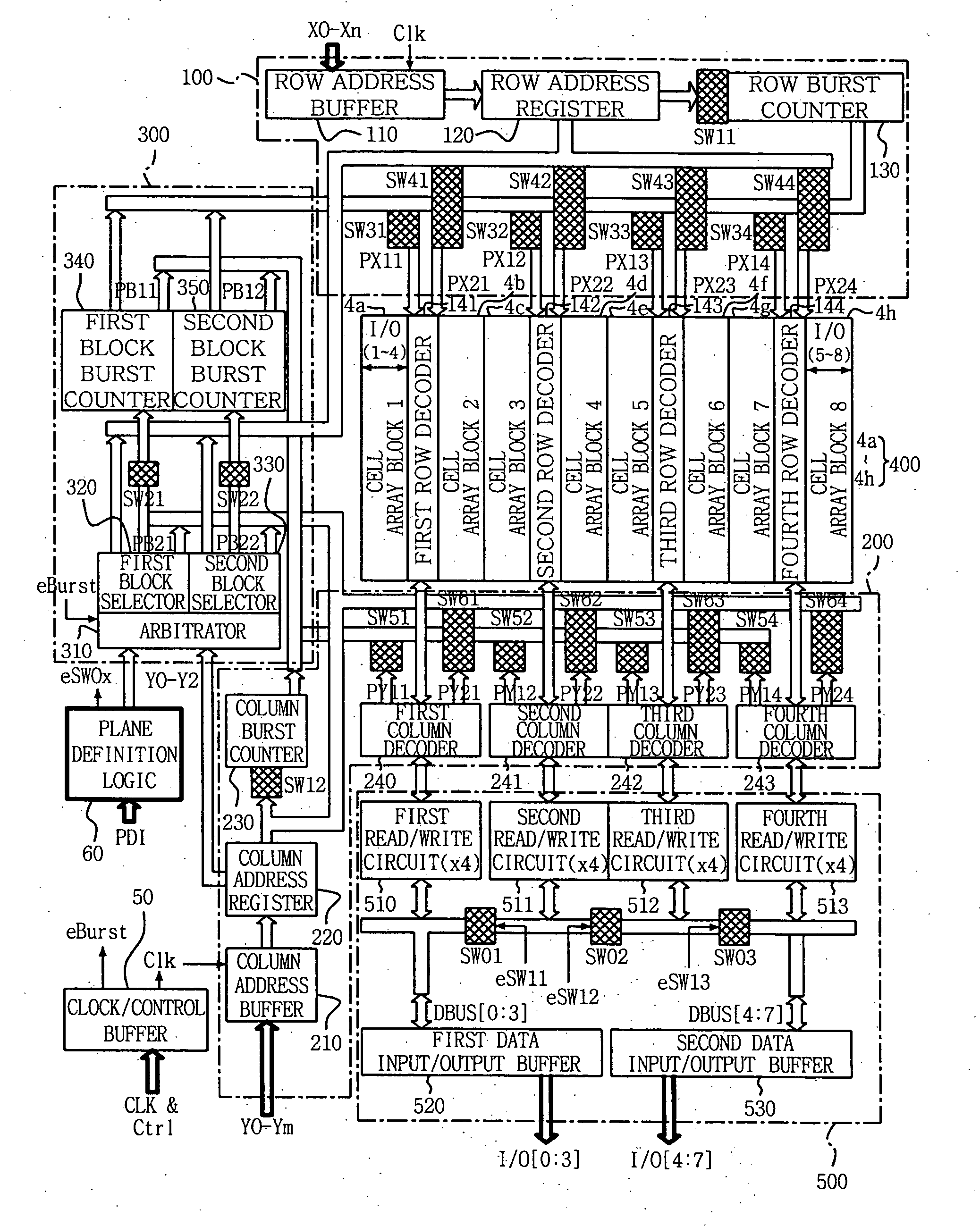
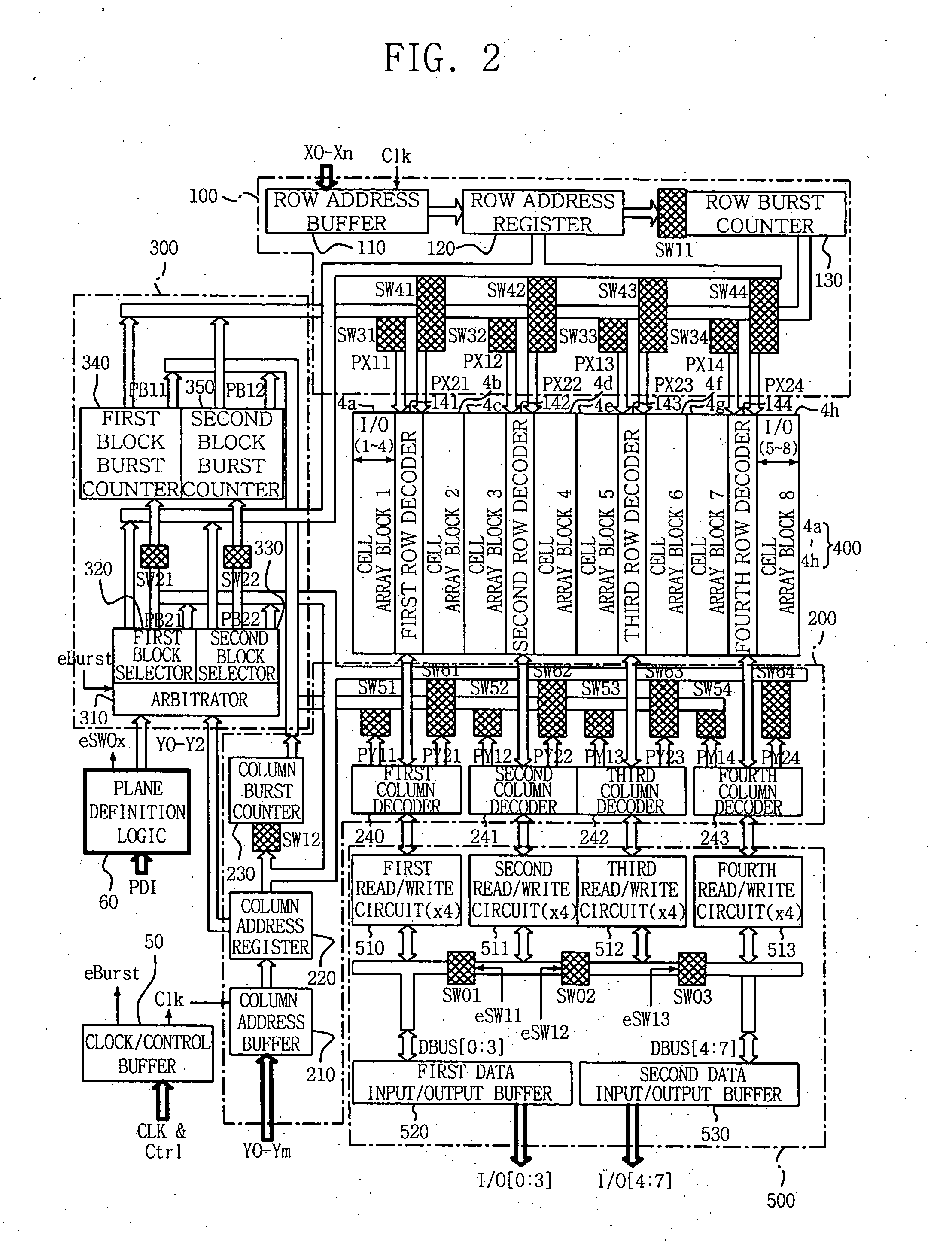
[0032]FIG. 2 is a circuit diagram illustrating a memory architecture for a semiconductor memory device according to one embodiment of the present invention. Referring to FIG. 2, a semiconductor memory device comprises a clock / control buffer 50, a plane definition logic unit 60, a row decoding path 100, a column decoding path 200, a block selection path 300, a memory cell array 400 including a plurality of cell array blocks 4a through 4h, and a read / write path 500. Row decoding path 100 should be viewed to include first through fourth row decoders 141-144 in addition to those elements shown within a broken box corresponding to row decoding path 100. Plane definition logic unit 60 and block selection path 300 collectively function as a memory plane de...


PUM

PropertyMeasurementUnit
impedanceaaaaaaaaaa
speedaaaaaaaaaa
processing speedaaaaaaaaaa

Abstract

A semiconductor memory device and a method of operating the semiconductor memory device are disclosed. The semiconductor memory device comprises a memory cell array having a plurality of cell array blocks. The cell array blocks are operationally divided into a plurality of memory planes using a memory determining unit. Each of the memory planes comprises at least one cell array block and is capable of executing independent data access operations using an independent operating mode.

Description

BACKGROUND OF THE INVENTION [0001] 1. Field of the Invention [0002] The present invention relates generally to a semiconductor memory device, and more particularly, to a high-speed semiconductor memory device such as Random Access Memory (RAM). [0003] A claim of priority is made to Korean Patent Application 10-2004-0031360 filed on May 4, 2004, the disclosure of which is hereby incorporated by reference in its entirety. [0004] 2. Description of the Related Art [0005] Semiconductor memory devices such as RAM typically function to store data in electronic systems. For example, a static random access memory (SRAM) is often used to store data transmitted or received between a host system such as central processing unit (CPU) or a digital signal processor (DSP) having a master function, and various peripheral devices having a slave function. SRAM is also used to store data for the host system in order to increase its overall processing speed. In such cases, the SRAM is used as a buffer m...

Claims


Application Information

Patent Timeline
Patent Type & Authority Applications(United States)
IPC IPC(8): G11C7/10G11C11/41G11C7/22G11C8/00G11C8/12G11C8/16
CPCG11C7/1042G11C8/16G11C8/12G11C7/22D03D1/08D03D15/00B23K26/402
Inventor SUH, YOUNG-HO
Owner SAMSUNG ELECTRONICS CO LTD
Why Eureka
Try Eureka