Thin-film transistor structure, method for manufacturing the thin-film transistor structure, and display device using the thin-film transistor structure

a thin film transistor and structure technology, applied in the direction of transistors, semiconductor devices, electrical devices, etc., can solve the problems of affecting the manufacturing yield of the display device, the resistance of the present gate wiring is difficult to achieve a high definition of 200 ppi or higher, and other wirings such as the signal wiring crossing the gate wiring are broken down, so as to achieve the effect of improving the manufacturing yield and low cos

Inactive Publication Date: 2005-11-10
INT BUSINESS MASCH CORP
View PDF5 Cites 28 Cited by
  • Summary
  • Abstract
  • Description
  • Claims
  • Application Information

AI Technical Summary

Benefits of technology

[0011] It is an object of the present invention to achieve a large screen and a high definition in a display device using a TFT at a low cost while solving problems regarding a propagation delay of a gate wiring and at the same time improving manufacturing yield.

Problems solved by technology

However, when studying a 30-inch display device, in which the material of very low resistivity such as the foregoing Cu is used and also a definition is measured on diagonal lines thereof under a condition that a switching speed of the TFT is ignored, it turns out to be difficult to achieve a high definition of 200 ppi or higher with resistivity of the present gate wiring.
Accordingly, a transmission delay of signals may occur.
Furthermore, though a thickness of the gate wiring can be simply increased, the mere increase in the thickness of the gate wiring causes another disadvantage that other wirings such as a signal wiring crossing the gate wiring are broken down.
Although it is possible to increase the thickness of the gate wiring significantly since a film growth rate is low in the conventional vapor deposition method such as the sputtering method, this method may cause disadvantages in manufacturing such as a low yield and a high cost.
However, any of the methods described above have not been satisfactory in terms of achieving a large screen, a high definition, an improved manufacturing yield and a reduced manufacturing cost while minimizing a propagation delay of a display device including a TFT structure.

Method used


Image

  • Thin-film transistor structure, method for manufacturing the thin-film transistor structure, and display device using the thin-film transistor structure
  • Thin-film transistor structure, method for manufacturing the thin-film transistor structure, and display device using the thin-film transistor structure
  • Thin-film transistor structure, method for manufacturing the thin-film transistor structure, and display device using the thin-film transistor structure

Examples


Embodiment Construction

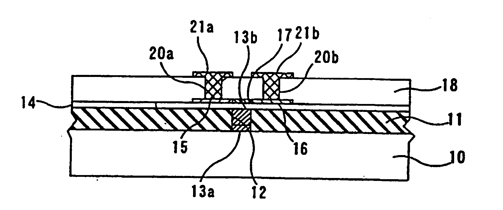
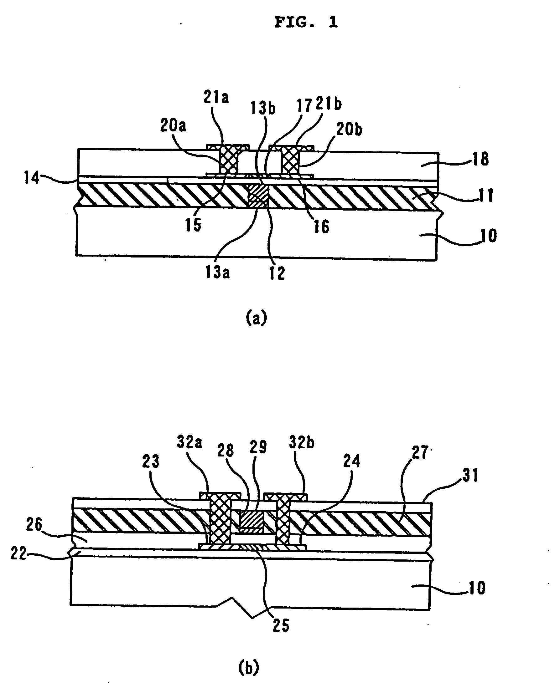
[0031] FIGS. 1(a) and 1(b) are drawings showing a TFT structure of the present invention. FIG. 1(a) shows a structure of a bottom gate type TFT, and FIG. 1(b) shows a structure of a top gate type TFT. In the TFT structure shown in FIG. 1(a), an insulating polymer film 11 is provided on a substrate 10 such as insulating glass and ceramics, and a gate wiring formed by a plurality of conductive layers 13a and 13b are buried in a trench 12 formed in the insulating polymer film 11. The insulating polymer film 11 that can be employed in the present invention may be constituted of any one of insulating polymer material and polymer composition.

[0032] As the polymer composition that can be used in the present invention, it is possible to enumerate, as specific examples, thermoplastic resin or thermosetting resin such as polyacrylate, polystyrene, polyacrylate styrene, polyester, epoxy resin, polycarbonate resin, polyamide resin and the like. The polymer material that can be used as the insu...


PUM


Abstract

The present invention provides a thin film transistor structure in which at least a trench is formed in an insulating polymer film formed on a substrate. In the thin film transistor structure, a trench formed in the insulating polymer film accommodates a gate wiring constituted of a plurality of conductive layers. Provided also are a method of manufacturing the thin film transistor structure, and a display device including a thin film transistor array composed of the thin film transistors constituted as described above.

Description

BACKGROUND OF THE INVENTION [0001] The present invention relates to a thin film transistor structure, a method of manufacturing the same and a display device including the same, more particularly to a thin film transistor capable of realizing a high definition display without causing a signal delay and providing a large display screen by making a gate wiring which is connected to the thin film transistor have a large cross sectional area while reducing floating capacitance, a method of manufacturing the same, and a display device including the same. [0002] A liquid crystal display using a thin film transistor (hereinafter referred to as a TFT) has been widely used as a display device in apparatuses such as computers, cellular telephones, watches and television sets to perform various displays. Particularly, a large screen and a high definition of a display device using the TFT have been demanded in recent years accompanied with increases in capability and storage capacitance of the ...

Claims


Application Information

Patent Timeline
Patent Type & Authority Applications(United States)
IPC IPC(8): H01L21/336H01L29/49H01L29/786
CPCH01L29/4908H01L29/78603H01L29/66765H01L29/66757H01L29/786
Inventor SUZUKISUEOKA, KUNIAKI
Owner INT BUSINESS MASCH CORP
Why Eureka
Try Eureka