Method and structure for implementing enhanced electronic packaging and PCB layout with diagonal vias

Inactive Publication Date: 2005-11-10
IBM CORP
View PDF7 Cites 22 Cited by
  • Summary
  • Abstract
  • Description
  • Claims
  • Application Information

AI Technical Summary

Benefits of technology

[0008] In accordance with features of the invention, diagonal vias are used to interconnect between a high-density pitch on the first side and a larger pitch on the opposite second

Problems solved by technology

Current via technology is limited to using only a single direction between a first side and an opposite

Method used


Image

  • Method and structure for implementing enhanced electronic packaging and PCB layout with diagonal vias
  • Method and structure for implementing enhanced electronic packaging and PCB layout with diagonal vias
  • Method and structure for implementing enhanced electronic packaging and PCB layout with diagonal vias

Examples


Embodiment Construction

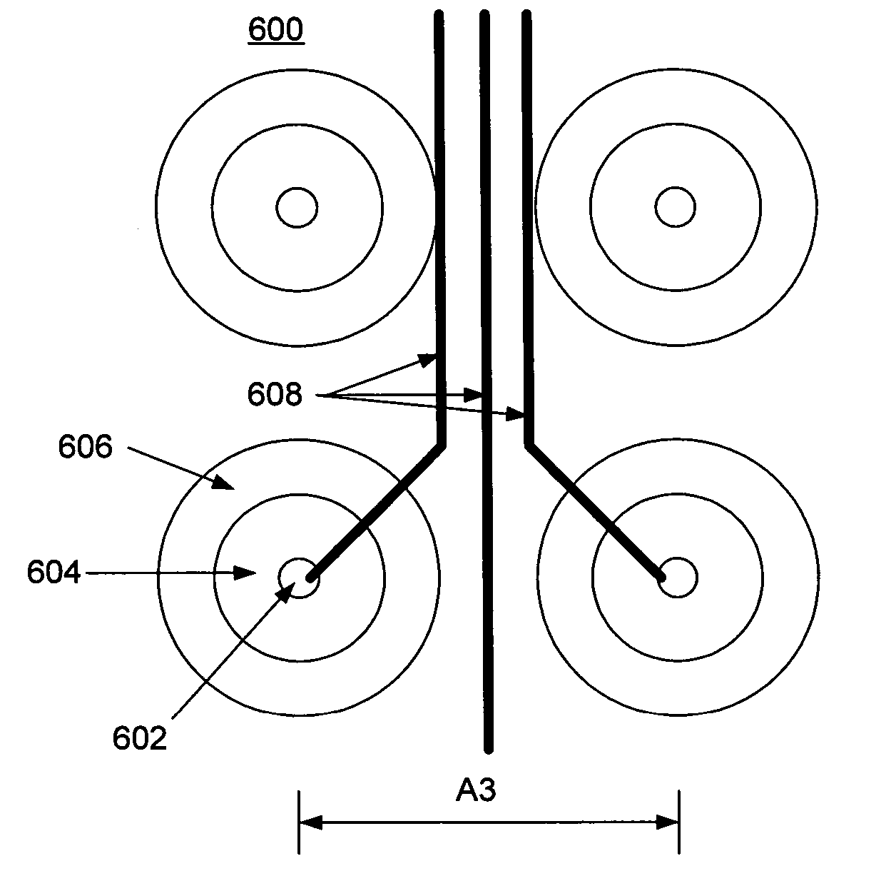
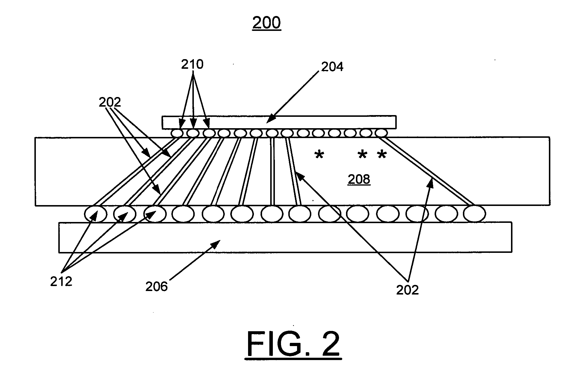
[0019] In accordance with features of the preferred embodiments, a diagonally arranged three-dimensional via or a diagonal via is provided for forming electrical connections for printed circuit boards (PCBs) and electronic packages. A laser can be used to drill holes or vias through a printed circuit board with the board tilted at a selected angle relative to the laser to form the diagonal vias. The diagonal vias are then plated with an electrically conductive material, such as copper to form electrical connections between layers. With the laser or board tilted at a variable angle, the diagonal vias formed are not perpendicular to the planar surface of the PCB. The diagonal vias enable optimization of wireability of packages in all three dimensions simultaneously.

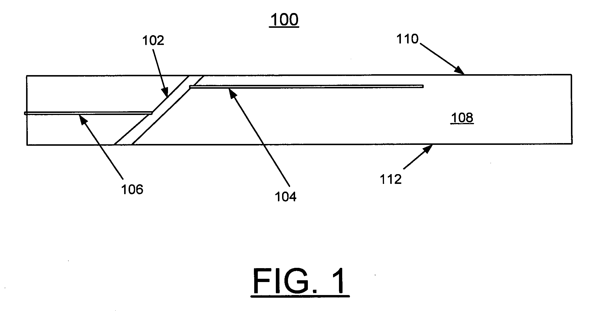
[0020] Having reference now to the drawings, in FIG. 1, there is shown an exemplary structure 100 including a diagonal via generally designated by the reference character 102 in accordance with the preferred embodiment. St...


PUM


Abstract

A method and structure are provided for implementing enhanced electronic packaging and printed circuit board (PCB) layout. A diagonal via is formed at a selected angle between a first side and an opposite second side of a printed circuit board at a selected printed circuit board location. The diagonal via is plated with an electrically conductive material. Diagonal vias are used to interconnect between a high-density pitch on the first side and a larger pitch on the opposite second side of the printed circuit board. The diagonal vias can be used to selectively interconnect electrical patterns of selected layers and eliminate the use of blind and buried vias.

Description

FIELD OF THE INVENTION [0001] The present invention relates generally to the data processing field, and more particularly, relates to a method and structure for implementing enhanced electronic packaging and printed circuit board (PCB) layout with diagonal vias. DESCRIPTION OF THE RELATED ART [0002] As used in the present specification and claims, the term printed circuit board or PCB means a substrate or multiple layers (multi-layer) of substrates used to electrically attach electrical components and should be understood to generally include circuit cards, printed circuit cards, printed wiring cards, and printed wiring boards. [0003] Electrical interconnection between electrically conductive paths of patterned copper in the various layers of multi-layer boards typically is accomplished through vias. The formation of the vias differs depending on the technology of the printed circuit board. Vias often are formed by drilling holes and plating the paths through the holes. The vias can...

Claims


Application Information

Patent Timeline
IPC IPC(8): G06F17/50H01L21/44H01L23/498H05K1/11H05K3/00H05K3/42
CPCH01L23/49827H01L2224/16H01L2924/01078H01L2924/15173H01L2924/15174H05K2201/09836H05K1/112H05K1/115H05K3/0032H05K3/429H01L2924/15311
Inventor BARTLEY, GERALD KEITHBECKER, DARRYL JOHNDAHLEN, PAUL ERICGERMANN, PHILIP RAYMONDMAKI, ANDREW B.MAXSON, MARK OWEN
Owner IBM CORP
Why Eureka
Try Eureka