Solar cell and its manufacturing method

a manufacturing method and solar cell technology, applied in the field of solar cells, can solve the problems of degrading the efficiency of solar cell modules, low conversion efficiency, and inability to manufacture integrated solar cells, and achieve excellent properties and reliability

Inactive Publication Date: 2005-11-17
PANASONIC CORP
View PDF1 Cites 89 Cited by
  • Summary
  • Abstract
  • Description
  • Claims
  • Application Information

AI Technical Summary

Benefits of technology

[0008] In light of the above, it is an object of the present invention to provide a solar cell with a

Problems solved by technology

However, when using a metal foil alone for a substrate, an integrated solar cell cannot be manufactured, because the metal foil has electrical conductivity.
However, since the insulation properties of the insulating layer were not sufficient, the conversion efficiency was as low as 6.0%.
In a solar cell module, when one of the unit cells is damaged, partly stained on its surface or partly shaded, the unit cell does not produce electric power, and accordingly the efficiency of the solar cell module is degraded.
Moreover, if the solar cell module in such a condition is exposed to sunshine for a long time, normally oper

Method used


Image

  • Solar cell and its manufacturing method
  • Solar cell and its manufacturing method
  • Solar cell and its manufacturing method

Examples


embodiment 1

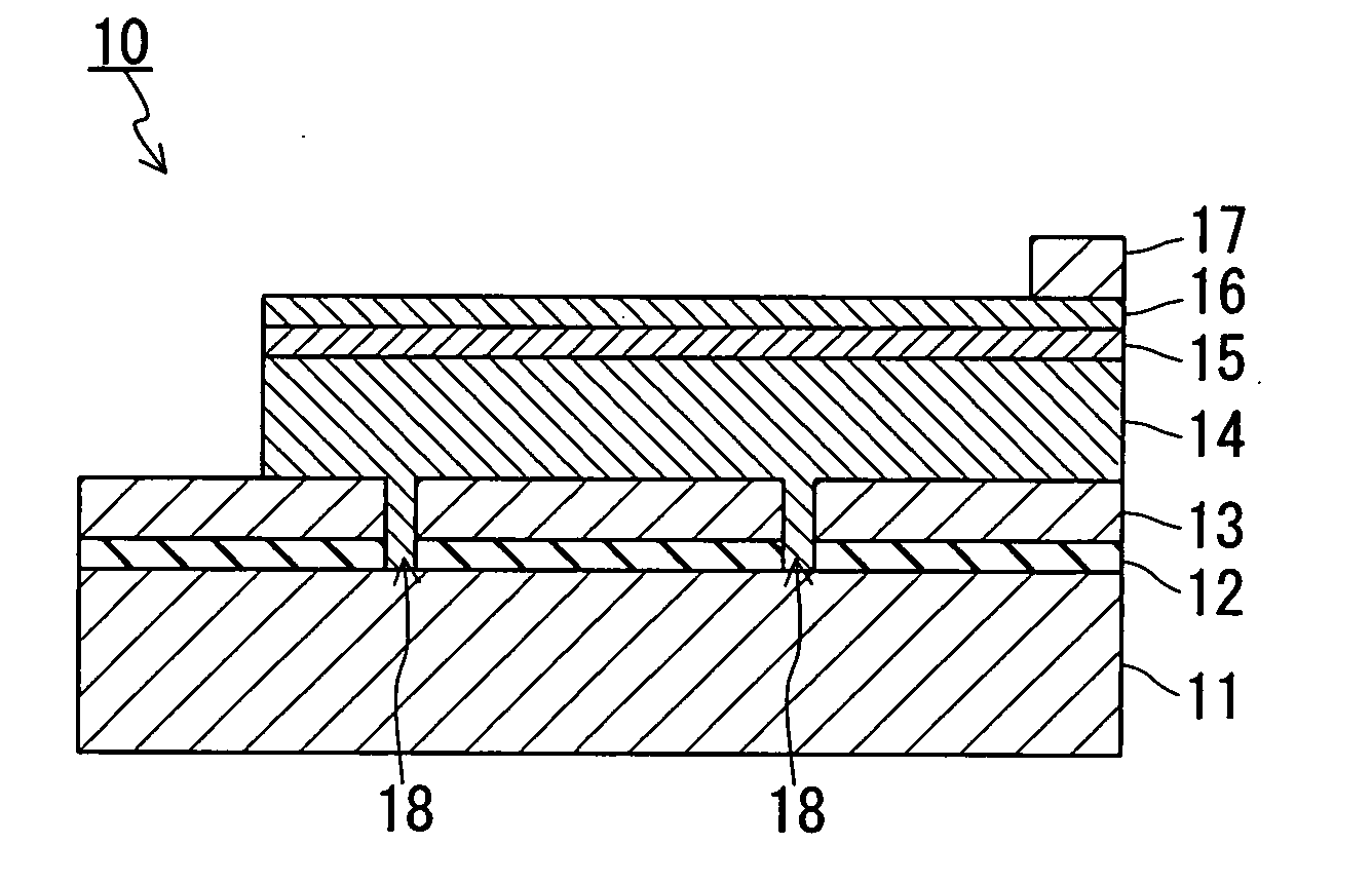
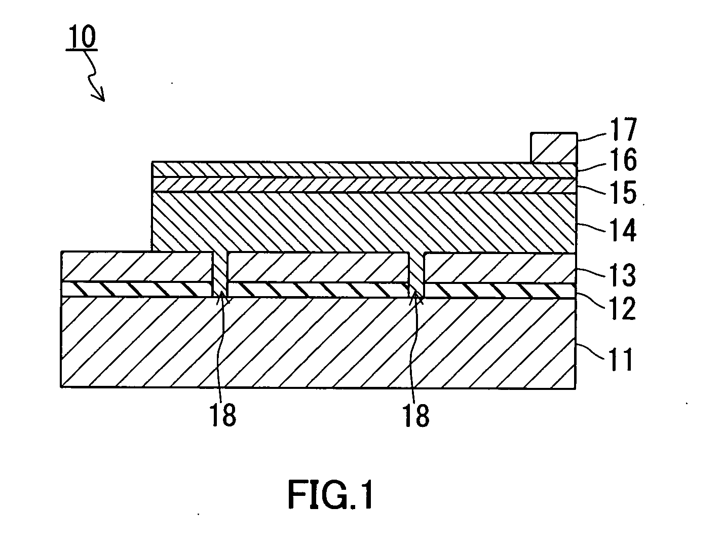
[0036] In Embodiment 1, an example of a configuration of a thin-film solar cell of the present invention will be described.

[0037] The cross-sectional view of a solar cell of Embodiment 1 is shown in FIG. 1. As shown in FIG. 1, a solar cell 10 of Embodiment 1 includes a conductive substrate 11, an insulating layer 12 formed on the conductive substrate 11, a conducting layer 13 formed on the insulating layer 12, a semiconductor layer 14 formed on the conducting layer 13, a window layer 15 formed on the semiconductor layer 14, a transparent conductive film 16 formed on the window layer 15, and an extraction electrode 17 formed on the transparent conductive film 16. Moreover, a second window layer made of a semiconductor or an insulator may be further provided between the window layer 15 and the transparent conductive film 16.

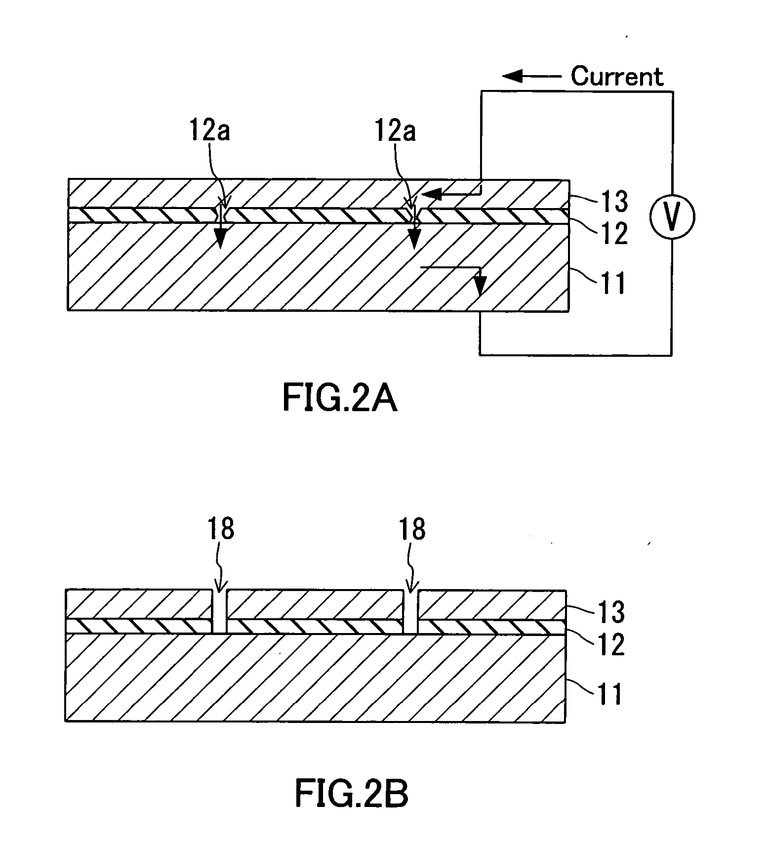
[0038] In the insulating layer 12 and the conducting layer 13, a through hole 18 is formed so as to penetrate them. The through hole 18 is filled with a semicond...

embodiment 2

[0054] In Embodiment 2, an example of a thin-film solar cell of the present invention will be described. More specifically, one example of an integrated solar cell module, in which plural solar cells (unit cells) are serially connected on a substrate, will be described.

[0055] The cross-sectional view of a solar cell module of Embodiment 2 is shown in FIG. 4. As illustrated in FIG. 4, a solar cell module 20 of Embodiment 2 includes a conductive substrate 21, an insulating layer 22 formed on the conductive substrate 21, a conducting layer 23 that functions as a backside electrode and is formed on the insulating layer 22, a semiconductor layer 24 that functions an optical absorption layer and is formed on the conducting layer 23, a window layer 25 made of a semiconductor or an insulator formed on the semiconductor layer 24, and a transparent conductive film 26 formed on the window layer 25. Moreover, a second window layer made of a semiconductor or an insulator further can be provided...

example 1

[0071] Example 1 is directed to a solar cell of Embodiment 1 and an example of a method for manufacturing the same.

[0072] A configuration of a solar cell 30 will be described, with reference to FIG. 6. In Example 1, a stainless substrate 31 (thickness: 50 μm) for the conductive substrate 11, a SiO2 layer 32 (thickness: 0.5 μm) for the insulating layer 12, a Mo layer 33 (thickness: 0.8 μm) for the conducting layer 13, a CIGS layer 34 (thickness: 2 μm) for the semiconductor layer 14 that functions as an optical absorption layer, a CdS layer 35a (thickness: 0.1 μm) for the first window layer of the window layer 15, a ZnO layer 35b (thickness: 0.1 μm) for the second window layer of the window layer 15, an ITO film 36 (thickness: 0.1 μm) for the transparent conductive film 16, and a laminating film 37 of NiCr / Al (overall thickness: 1.5 μm) for the extraction electrode 17 were used.

[0073] Next, a method for manufacturing a solar cell is described as follows. Firstly, a SiO2 layer 32 was...


PUM


Abstract

A solar cell includes a conductive substrate, and an insulating layer, a conducting layer and a semiconductor layer that are disposed on the substrate. A through hole is formed so as to penetrate the insulating layer and the conducting layer, and the through hole is filled with a semiconductor that composes the semiconductor layer. At least one element selected from the elements composing the conductive substrate diffuses into the semiconductor with which the through hole is filled.

Description

TECHNICAL FIELD [0001] The present invention relates to a solar cell and a method for manufacturing the same. BACKGROUND ART [0002] A thin-film solar cell using CuInSe2 (CIS) or Cu(In, Ga)Se2 (CIGS) that is a solid solution of CIS with Ga, as a optical-absorption layer (hereinafter, it may be called as a CIS solar cell or a CIGS solar cell, respectively), is known. CIS and CIGS are compound semiconductor layers (chalcopyrite structured semiconductor layers) comprising elements from each of groups Ib, IIIB and VIb. It is reported that such a CIS solar cell and a CIGS solar cell have an advantage of showing a high energy conversion efficiency and being free from a deterioration of efficiency caused by irradiation with light. [0003] Since a CIS solar cell and a CIGS solar cell can be formed by laminating thin films, they can be formed on a flexible substrate, and an integrated solar cell can be manufactured by forming a plurality of serially connected unit cells on a substrate. In orde...

Claims


Application Information

Patent Timeline
IPC IPC(8): H01L31/04H01L21/36H01L31/0256H01L31/042
CPCY02E10/541H01L31/042H01L31/0443H01L31/046Y02P70/50
Inventor NEGAMI, TAKAYUKISHIMAKAWA, SHINICHISATOH, TAKUYAHAYASHI, SHIGEO
Owner PANASONIC CORP
Why Eureka
Try Eureka