Semiconductor device structure with adhesion-enhanced semiconductor die

a technology of semiconductor dies and dies, which is applied in the direction of semiconductor devices, semiconductor/solid-state device details, electrical equipment, etc., can solve the problems of difficult to obtain a good, solid adhesive bond between the die and the package, the oxide on the silicon die substrate does not lend itself to uniform wetting, and the surface of other problems, to achieve the effect of reducing the delamination potential of the die, reducing the cracking of the package, and improving the adhesion of the di

Inactive Publication Date: 2005-11-17
KING JERROLD L +2
View PDF29 Cites 2 Cited by
  • Summary
  • Abstract
  • Description
  • Claims
  • Application Information

AI Technical Summary

Benefits of technology

[0016] Advantageously, the metal layer on the die provides a uniform wetting surface for better adhesion of the die with the mold compound during encapsulation. The increased adhesion reduces delamination potential of the die from the package and, consequently, reduces cracking of the package.

Problems solved by technology

Although IC packaging is minimized in each of these packaging techniques that uses an adhesive tape, other problems surface.
One such problem in the LOC technique is the difficulty of obtaining a good, solid adhesive bond between the die and the package.
One reason a solid bond is not achieved is because the oxide on the silicon die substrate does not lend itself to uniform wetting, which is necessary for good adhesion with the liquid mold compound.
When a die does not bond well with the mold compound package, delamination may occur and the device may potentially be ruined during the manufacturing process or surface mount of the package.
When the moisture is converted to steam from heat processes and the steam pressure is greater than the strength of the adhesion couple between the mold compound and the die, the mold compound will crack or explode with a “popcorn” effect.
Although these techniques are commonly used in the semiconductor industry, they provide only a temporary solution.
Namely, when a semiconductor manufacturer ships a “dried” packaged device by following these techniques, the device may still absorb moisture at a customer's site after the device is removed from the shipping container materials.
Furthermore, if the die has delaminated even slightly, the package is subject to moisture penetration again and the package may subsequently crack if exposed to sufficient heat.
Although this method provides a working solution, it retains disadvantages by its use of aminopropyltriethox-silane as a coating on the die.
Obviously, the foregoing problems and solutions associated with providing a good bond between a die and a die package to avoid delamination and cracking of the package are undesirable aspects of conventional semiconductor packaging techniques.

Method used


Image

  • Semiconductor device structure with adhesion-enhanced semiconductor die
  • Semiconductor device structure with adhesion-enhanced semiconductor die

Examples


Embodiment Construction

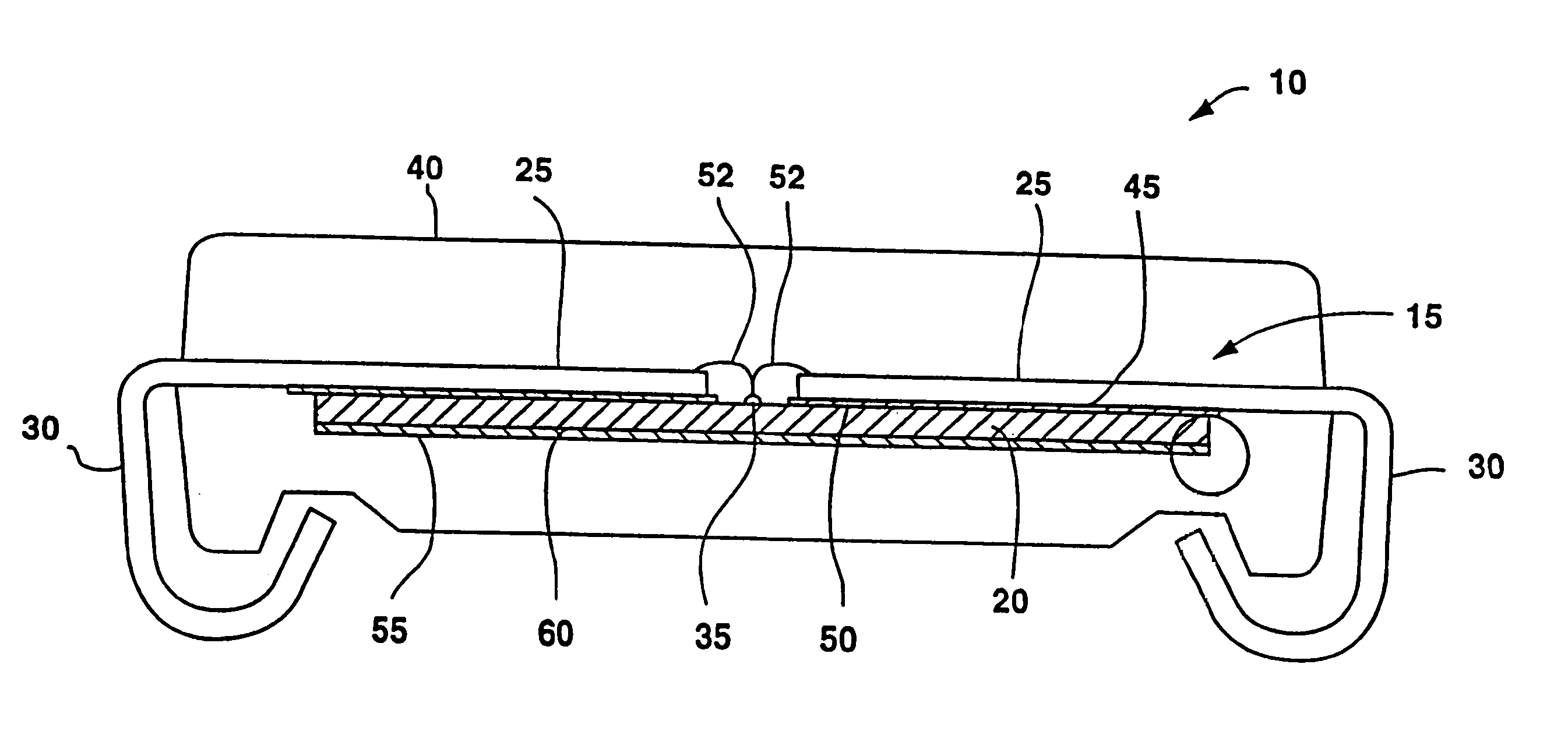
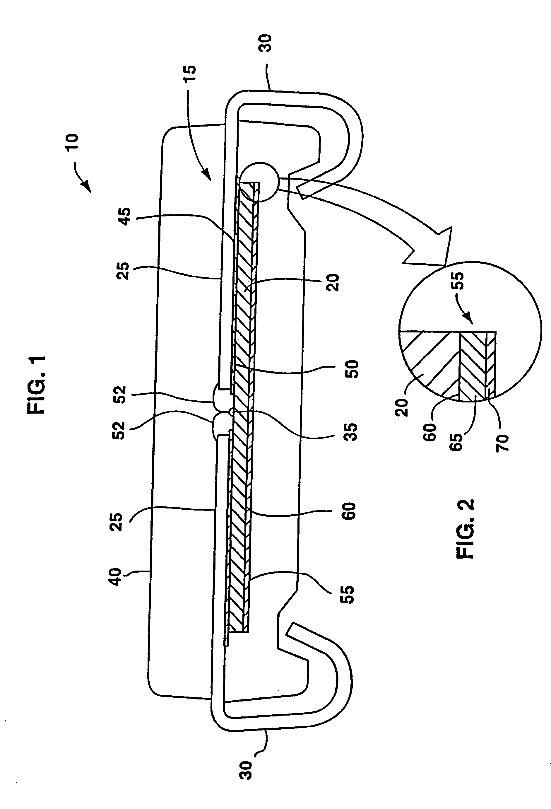
[0020]FIG. 1 is an end-section view of packaged integrated circuit (IC) 10. Lead frame 15 is disposed over IC die 20, the lead frame including inner and outer lead finger portions 25 and 30, respectively. Inner lead finger portions 25 are adjacent die pads 35, and outer lead finger portions 30 extend outward of mold compound packaging 40 for connection with appropriate external circuitry.

[0021] Insulator adhesive tape strips 45 are disposed between inner lead finger portions 25 and frontside 50 of die 20 to adhere the lead finger portions to the die. Integrated circuitry is disposed on frontside 50 of die 20. Wire bonds 52 communicate between inner lead finger portions 25 and die pads 35 for making the electrical connection between the die and the lead finger portions.

[0022] Metal layer 55 is shown deposited over back side 60 of die 20. Metal layer 55 enhances adhesion of die 20 with mold compound packaging 40. Metal layer 55 is deposited over die 20 using an electroplating proces...


PUM

PropertyMeasurementUnit
humidityaaaaaaaaaa
adhesionaaaaaaaaaa
thicknessaaaaaaaaaa

Abstract

A semiconductor die includes a substantially oxide-free metal layer on at least a portion of a surface thereof. The substantially oxide-free metal may enhance adhesion of a packaging material, or mold compound, to the semiconductor die, prevent the occurrence of voids or presence of moisture between the packaging material and the adjacent surface of the semiconductor die, or otherwise prevent delamination of the packaging material from the adjacent surface of the semiconductor die. The substantially oxide-free metal may be copper, palladium, another substantially oxide-free metal, or a combination of substantially oxide-free metals.

Description

CROSS-REFERENCE TO RELATED APPLICATIONS [0001] This application is a divisional of application Ser. No. 10 / 852,632, filed May 24, 2004, pending, which application is a continuation of application Ser. No. 10 / 309,643, filed Dec. 3, 2002, now U.S. Pat. No. 6,740,545, issued May 25, 2004, which is a continuation of application Ser. No. 09 / 873,581, filed Jun. 4, 2001, now U.S. Pat. No. 6,489,186, issued Dec. 3, 2002, which is a continuation of application Ser. No. 09 / 394,180, filed Sep. 10, 1999, now U.S. Pat. No. 6,316,292, issued Nov. 13, 2001, which is a continuation of application Ser. No. 08 / 963,395, filed Nov. 3, 1997, now U.S. Pat. No. 6,066,514, issued May 23, 2000, which is a divisional of application Ser. No. 08 / 731,793, filed Oct. 18, 1996, now U.S. Pat. No. 5,760,468, issued Jun. 2, 1998, which is a continuation of application Ser. No. 08 / 306,024, filed Sep. 14, 1994, now U.S. Pat. No. 5,583,372, issued Dec. 10, 1996.BACKGROUND OF THE INVENTION [0002] 1. Field of the Inventi...

Claims


Application Information

Patent Timeline
Patent Type & Authority Applications(United States)
IPC IPC(8): H01L23/31H01L23/495
CPCH01L23/3142H01L23/4951H01L24/48H01L2224/32245H01L2924/10253H01L2924/1815Y10S438/926Y10S438/928H01L2224/32014H01L2224/48091H01L2224/48247H01L2224/4826H01L2224/48465H01L2224/73215H01L2924/0102H01L2924/01029H01L2924/01046H01L2924/01078H01L2924/14H01L2924/1532H01L2924/00014H01L2924/00H01L2224/05599H01L2224/85399H01L2924/181H01L2224/45099H01L2224/45015H01L2924/207
Inventor KING, JERROLD L.BROOKS, J. MIKEMODEN, WALTER L.
Owner KING JERROLD L
Why Eureka
Try Eureka