

Inspection of TFT LCD panels using on-demand automated optical inspection sub-system
a technology of automatic inspection and optical inspection, applied in the direction of optical inspection of flaws/contamination, instruments, measurement devices, etc., can solve the problems of insufficient detection of defects, short circuit, foreign particles, over- and under-etching, etc., and achieve the effect of improving automatic inspection and accurately locating
- Summary
- Abstract
- Description
- Claims
- Application Information
AI Technical Summary
Benefits of technology
Problems solved by technology
Method used
Image

Examples
Embodiment Construction
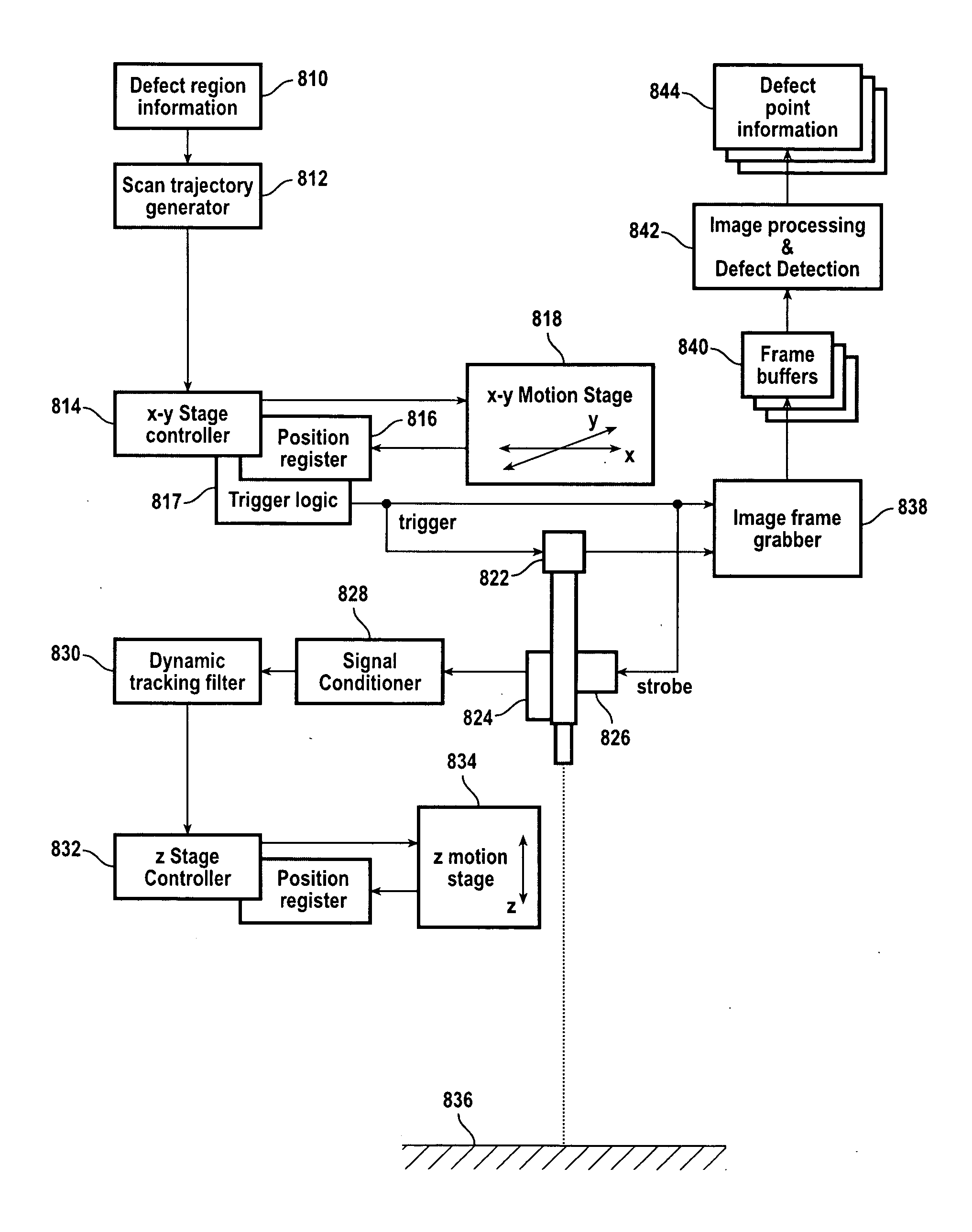
[0052] In an inspection system or in a group of systems consisting of inspection and repair equipment, a well defined process is used to determine how exactly the inspection and the subsequent optional repair operations will be performed. This process describes the roles of the sub-systems involved in the inspection and repair operations and the sequence of actions which will be performed on the article being inspected.
[0053] The present invention proposes to augment the instruments to add an improvement employing an AOI-on-demand sub-system.
[0054] The improved flow and added abilities to quickly identify defects with the added sub-system are considered to be a primary contribution of the present invention.
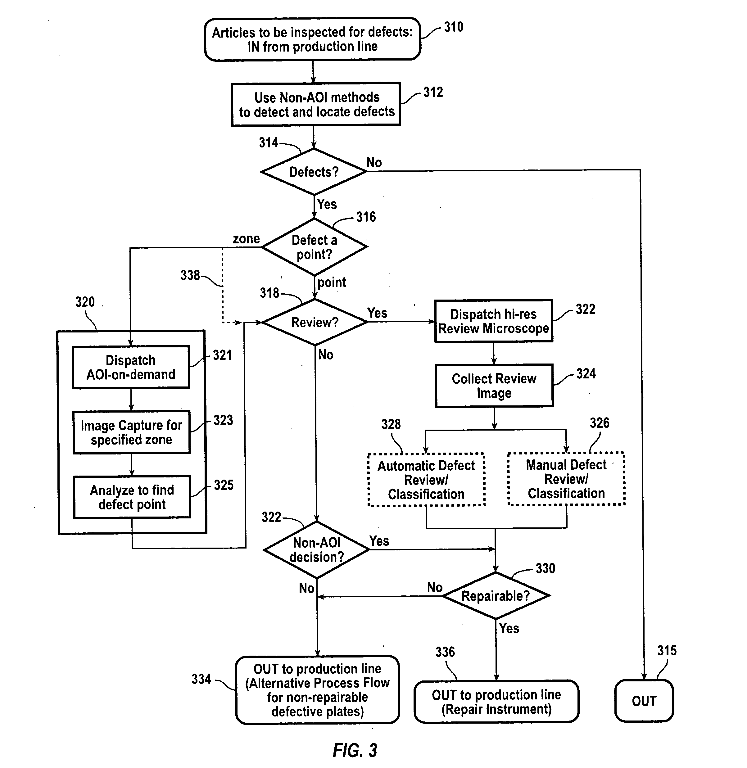
[0055] In FIG. 3, a specific embodiment of the AOI-on-demand process is presented where the new functionality is integrated into the inspection side of the process and into an inspection instrument. Articles subject to defect inspection are input (Step 310) to an inspection ins...
PUM
| Property | Measurement | Unit |
|---|---|---|
| speed | aaaaa | aaaaa |
| speed | aaaaa | aaaaa |
| speed | aaaaa | aaaaa |
Abstract
Description
Claims
Application Information