Method of manufacturing semiconductor device

a manufacturing method and semiconductor technology, applied in semiconductor devices, semiconductor/solid-state device details, electrical devices, etc., can solve the problems of less suitable resin substrates for interposers, difficulty in forming electrodes on resin substrates to correspond, and inability to meet the accuracy of pads, etc., to achieve easy and efficient cutting and division, and reduce the thickness of semiconductor substrates

Inactive Publication Date: 2005-11-17
SHINKO ELECTRIC IND CO LTD
View PDF1 Cites 73 Cited by
  • Summary
  • Abstract
  • Description
  • Claims
  • Application Information

AI Technical Summary

Benefits of technology

[0023] Grinding the back surface of the semiconductor substrate reduces the thickness of the semic...

Problems solved by technology

This is because pads on semiconductor elements are highly accurately formed by a wafer process whereas external connection terminals only need to be accurate enough to satisfy pitch based on wiring rules and therefore do not have accuracy as high as the accuracy of the pads.
However, as density of semiconductor elements grows and their size decreases, it is becoming difficult to form electrodes on a resin substrate to correspond to pads of semiconductor elements due to an accuracy difference between the semiconductor elements and the resin substrate.
As a result, res...

Method used


Image

  • Method of manufacturing semiconductor device
  • Method of manufacturing semiconductor device
  • Method of manufacturing semiconductor device

Examples


Embodiment Construction

[0041] A preferred embodiment of the present invention is described hereinafter with reference to the accompanying drawings.

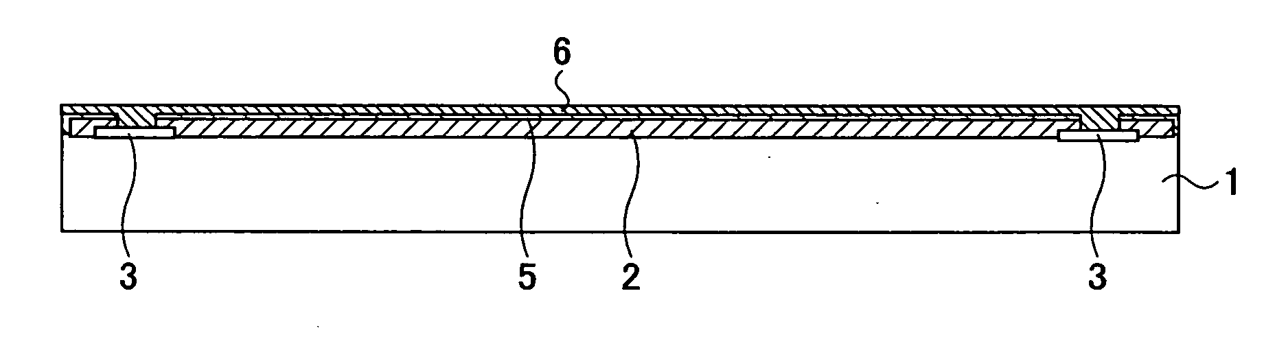
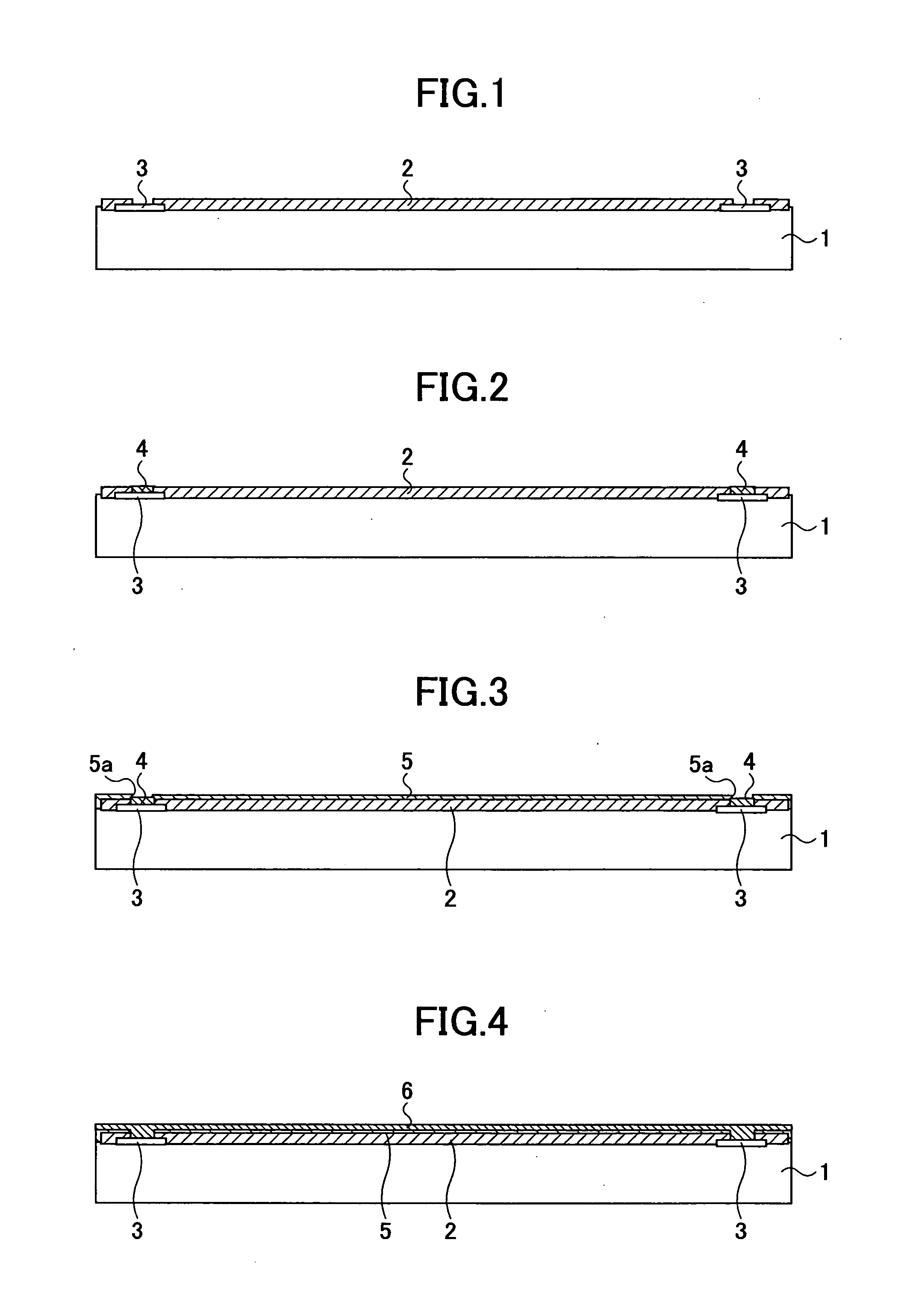
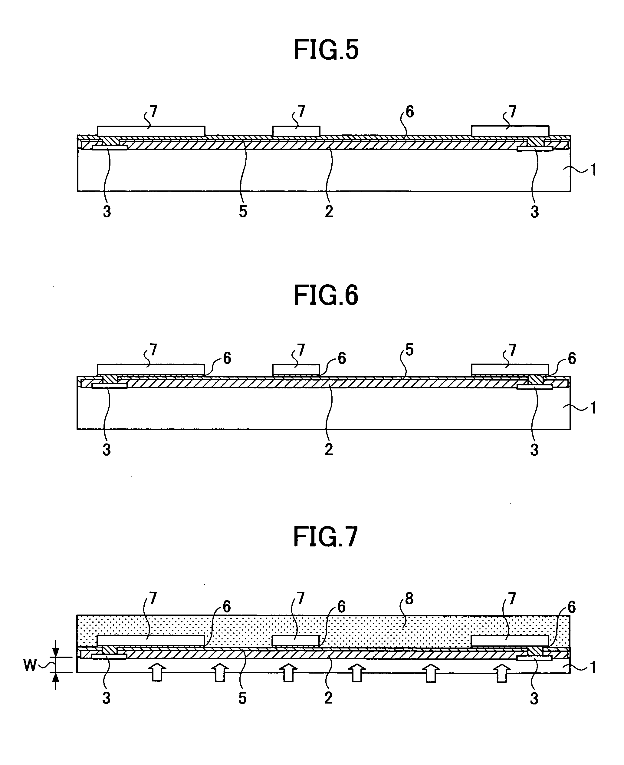
[0042]FIGS. 1 through 17 illustrate a method of manufacturing a semiconductor device as an embodiment of the present invention step by step. According to the method of manufacturing a semiconductor device of the present invention, a semiconductor substrate 1 as shown in FIG. 1 is used.

[0043] The semiconductor substrate 1 is a silicon wafer (hereinafter referred to as wafer 1) having plural semiconductor elements formed in advance. Each of the semiconductor elements serves as, for example, a memory. Aluminum electrodes 3 are formed on the outer side of an element area. A passivation film is formed on a front surface (element forming surface) of the wafer 1 except the area where the aluminum electrodes 3 are formed. The passivation film 2 may include silicon nitride (Sin) film.

[0044] Although the plural semiconductor elements are formed on the wafer 1, FIGS. 1...


PUM


Abstract

A method of manufacturing a semiconductor device having a build-up layer for wiring between semiconductor elements and external connection terminals is disclosed. The method comprises steps of forming a rewiring layer on a wafer, placing the wafer on a stretchable dicing tape, dicing the wafer placed on the dicing tape, forming a clearance between adjacent semiconductor elements by stretching the dicing tape, forming a semiconductor device continuous body by forming a build-up layer on the semiconductor elements and the clearance, and forming semiconductor devices by dicing the semiconductor device continuous body.

Description

BACKGROUND OF THE INVENTION [0001] 1. Field of the Invention [0002] The present invention relates to a method of manufacturing a semiconductor device, and particularly relates to a method of manufacturing a semiconductor device having a build-up layer for wiring between semiconductor elements and external connection terminals. [0003] 2. Description of the Related Art [0004] In recent years, LSI technologies as a key technology for multimedia devices have been steadily advanced to improve data transmission speed and capacity. With the advancement of the LSI technologies, high-density mounting techniques for interfaces between LSIs and electronic devices have also been developed. Among semiconductor packages, CSPs (Chip Size Package), whose size is substantially equal to the chip size, can offer high-density mountability. [0005] Although there are a variety of types of CSPs, most of the CSPs are configured to have an interposer between semiconductor elements and connection terminals (...

Claims


Application Information

Patent Timeline
IPC IPC(8): H01L21/00H01L23/52H01L21/3205H01L21/4763H01L21/56H01L21/60H01L21/68H01L21/78H01L23/12H01L23/31H01L23/498H01L23/525H01L23/538
CPCH01L21/56H01L21/568H01L2924/30105H01L2924/19041H01L2924/15311H01L21/6835H01L21/6836H01L21/78H01L23/3114H01L23/49816H01L23/525H01L23/5389H01L24/19H01L24/82H01L24/97H01L2221/68327H01L2221/68336H01L2221/6834H01L2224/18H01L2224/82039H01L2224/97H01L2924/01013H01L2924/01029H01L2924/01033H01L2924/01046H01L2924/01074H01L2924/01078H01L2924/01079H01L2924/01082H01L2924/14H01L2224/82H01L2924/01006H01L2924/014H01L2924/18162H01L2224/12105H01L2924/12042H01L2224/05024H01L2224/05008H01L2224/05022H01L2224/05567H01L2224/05001H01L2224/05124H01L2224/05147H01L2224/05155H01L2224/05644H01L2224/05655H01L2224/04105H01L2224/94H01L24/03H01L24/05H01L2924/00H01L2924/00014H01L2224/0214H01L23/12
Inventor YAMANO, TAKAHARUKURASHIMA, NOBUYUKI
Owner SHINKO ELECTRIC IND CO LTD
Why Eureka
Try Eureka