Sensor element for providing a sensor signal, and method for operating a sensor element

a sensor signal and sensor element technology, applied in the field of electronic semiconductor sensors, can solve the problems of dc voltage amplifiers suffering from offset problems, hall probes also suffering from relatively large offsets, and disruptive, in particular offset drifts, so as to reduce the offset, reduce the energy consumption, and reduce the effect of the offs

Active Publication Date: 2005-11-24
INFINEON TECH AG
View PDF3 Cites 37 Cited by
  • Summary
  • Abstract
  • Description
  • Claims
  • Application Information

AI Technical Summary

Benefits of technology

[0041] The present invention is based on the findings that by means of a favorable segmentation of individual phases with the spinning-current principle, frequent switching between the contact terminals of the measuring element may be avoided. While with the spinning-current principle, a measuring current is applied, as a controlled variable, to the individual contact terminals of the measuring element, for example in a clockwise or in a counter-clockwise manner, the inventive approach envisages that the controlled variable, i.e. the control current, is initially fed to the measuring element in a first direction between two contact terminals, and that in a second measuring phase, the control current is fed to the measuring element in the opposite direction at the same contact terminals. This is followed by a “switching”, i.e. by applying the control current to the measuring element at two further contact terminals, different from the first two contact terminals, in third and fourth measuring phases, it being possible again, in the third measuring phase, for the controlled variable to be applied to the measuring element in the first direction, and for the controlled variable to be applied to the measuring element, in the fourth measuring phase, in the direction which runs opposite to the direction of the controlled variable in the third measuring phase. Such a measuring approach enables a measuring variable to be measured at a measuring element without having to switch the contact terminals used as measuring contacts. Rather, by switching the direction of the controlled variable in the measuring element, the same effect may be achieved as if the measuring element is measured through in the clockwise or counter-clockwise direction (as in the prior art). To ensure that the measuring values detected are taken into account in a manner which is correct in terms of signs, the measuring signal then is to be determined on the basis of a difference between the first two measuring values and a difference between the third and fourth measuring values. The necessity of forming a difference results, in particular, from the fact that by reversing the controlled-variable direction in the measuring element while maintaining the measuring direction at the contact terminals used as measuring points, in a conventional spinning-current approach, the signs of the measuring values are reversed—as opposed to the prior art.
[0042] In contrast to the prior art, the inventive approach offers the advantage that by avoiding frequent switching of the contact terminals used as measuring contacts, a glitch energy may be reduced when a measuring signal is applied to the contact terminals. This results from the fact that switching the contact terminals leads, for example, to a reversal of the charge of parasitic capacitances of the measuring element, which is why, during reversal of the charge of the parasitic effects of the measuring element, energy pulses are formed which lead to measuring errors which, summed up, may make a considerable contribution to the offset of the measurement. In other words, this means that reversing the polarity of the controlled variable, as opposed to conventional switching, advantageously leads to no big common-mode signal jumps at the input of a chopper amplifier, since the voltage tappings remain at roughly the same potential when the supply terminals of the probe are switched. By maintaining constant the potential of the voltage tappings in this manner, a charge carrier injection, and thus charge-reversal energy, into the measuring element may be reduced, which results in a reduction of the offset in measuring with the measuring element, since the offset includes, among other things, averaging of the interference energy introduced during the measurement. By means of such a reversal of the polarity of the controlled variable (as opposed to re-clamping) at a constant switch position for tapping the measurement values, less energy therefore needs to be spent on recharging parasitic effects.

Problems solved by technology

In most cases, DC voltage amplifiers suffer from the offset problem, i.e. the fact that even with short-circuited input terminals, the output provides a signal different from zero, even though the ideal transfer function should be Ua=G·Ue, wherein Ua is the output voltage of the DC voltage amplifier, G is the amplification factor of the DC voltage amplifier, and Ue is the input voltage of the DC voltage amplifier.
In addition to the offset, what is also disruptive, in particular, is an offset drift.
Hall probes also suffer from a relatively large offset, i.e. with a fading magnetic field, they still provide an output voltage.
The reasons, in particular, of the offset drift which cannot be matched since it is unpredictable, lie predominantly in mechanical stress which disrupts the inherent symmetry of the probe by anisotropic conductivity which has been induced.
In practice, asymmetric charge injection has an adverse effect on such a chopper amplifier.
This leads to an error term superimposed on the signal.
In particular for high chopper frequencies, the errors become large, since with each clock pulse edge, charge is injected into the signal path.
This could be eliminated if it were possible to reduce the chopper frequency; this conflicts with the fact that at low frequencies, modulation noise becomes dominant and may thus ruin the improvements achieved by a reduction of the chopper frequency.
However, this causes the problem that for a good selection, the band pass should have a high quality; in this case, however, the signal being compromised, in the case of variations of the band-pass parameters, and thus not being transmitted with a precisely defined amplification factor.
However, even with such spinning-current Hall probes, practice sets a limitation, since it is only for electrically linear systems that this principle works perfectly well.
P. J. A. Munter presents a spinning-current Hall probe which, however, introduces a large amount of glitch energy into the Hall probe due to the frequent switching between gate terminal contacts and measuring contacts, which results in a comparatively large offset of the Hall probe.
With high magnetic sensitivities, the offset performance of simple chopper amplifiers and of simple spinning-current systems is not sufficient, as is shown by the following example.

Method used


Image

  • Sensor element for providing a sensor signal, and method for operating a sensor element
  • Sensor element for providing a sensor signal, and method for operating a sensor element
  • Sensor element for providing a sensor signal, and method for operating a sensor element

Examples


Embodiment Construction

[0048] In the following description of the preferred embodiments of the present invention, identical or similar reference numerals will be used for those elements depicted in the various drawings which have similar actions, a repeated description of these elements being omitted.

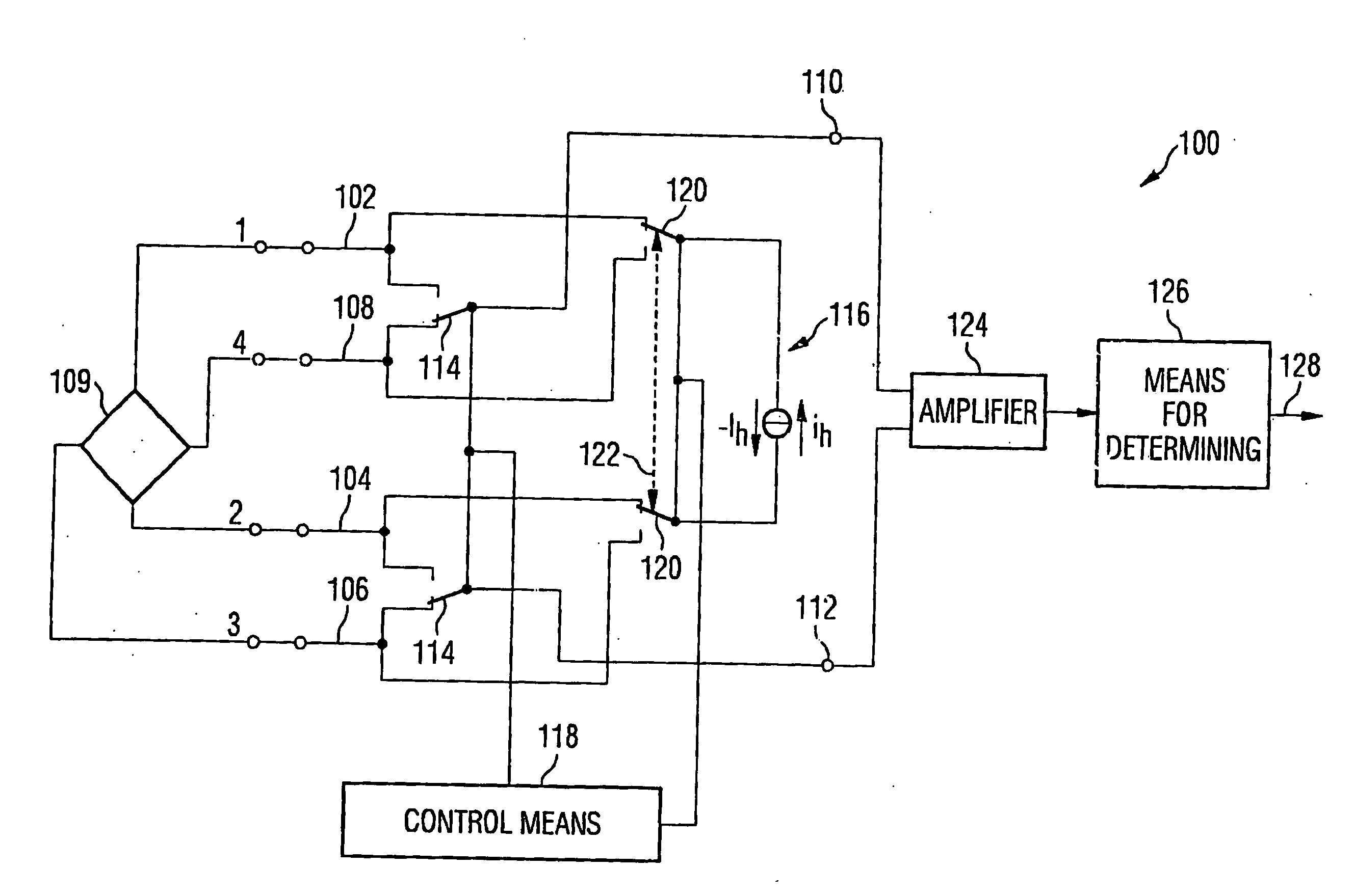
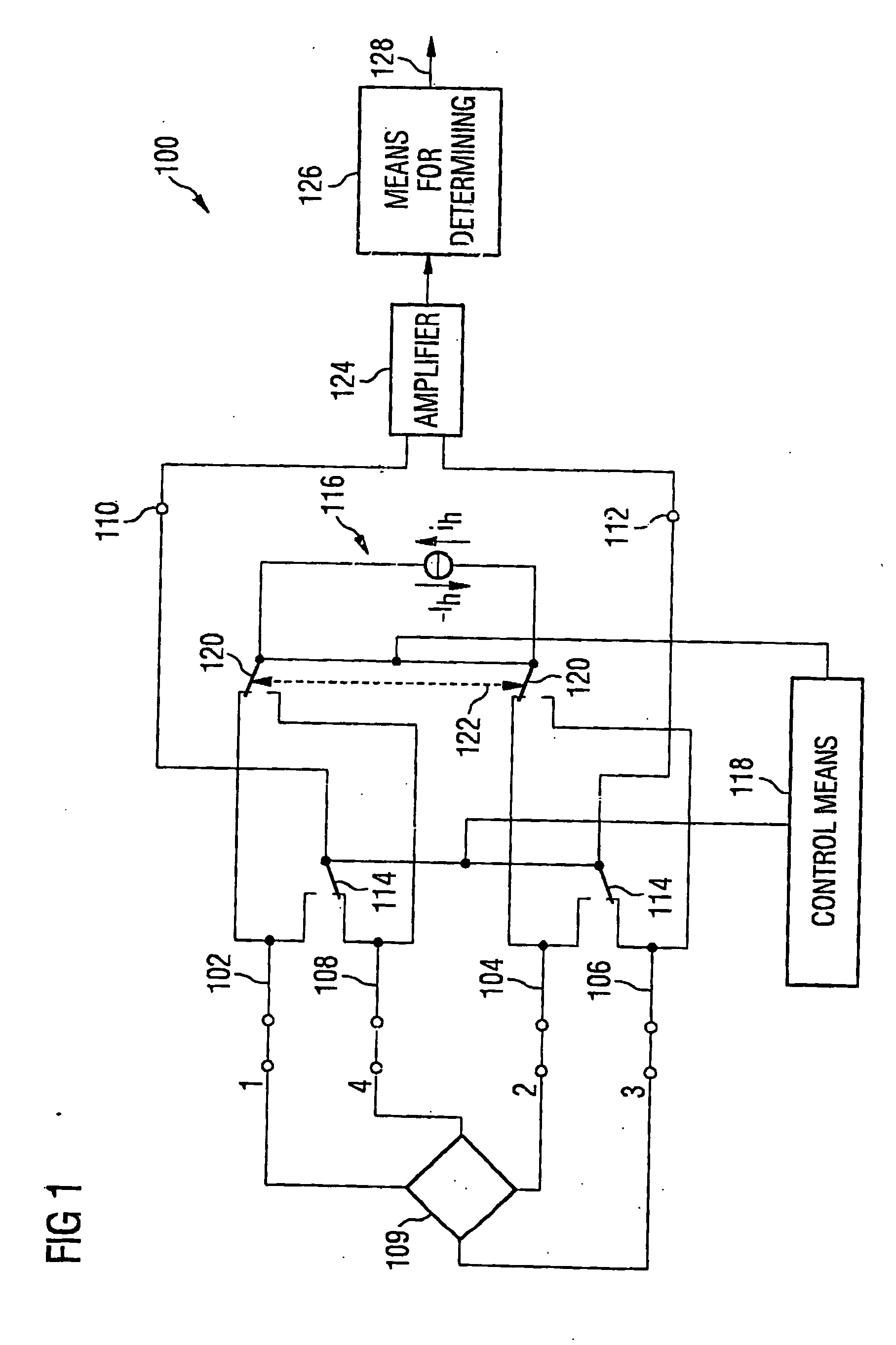
[0049]FIG. 1 shows a block diagram of an embodiment of an inventive sensor element 100. The sensor element 100 includes a first contact terminal 102, a second contact terminal 104, a third contact terminal 106, and a fourth contact terminal 108. In addition, sensor element 100 includes a measuring element 109 which may be connected to the first contact terminal 102 via a first terminal, to the second contact terminal 104 via a second terminal, to the third contact terminal 106 via a third terminal, and to the fourth contact terminal 108 via a fourth terminal. In addition, the sensor element includes a first output terminal 110 and a second output terminal 112. Furthermore, the sensor element 100 has a switch...


PUM


Abstract

A method for operating a sensor element having two contact terminal pairs, comprises steps of providing a first measurement value by applying a first controlled variable having a first polarity between the first terminal pair, and coupling the second terminal pair with output terminals; providing a second measurement value by applying a second controlled variable, having an opposed polarity, between the first terminal pair, and coupling the second terminal pair to the output terminals; providing a third measurement value by applying the first variable between the second terminal pair, and coupling the first terminal pair with the output terminals, providing a fourth measurement value by applying the second variable between the second terminal pair, and coupling the first terminal pair with the output terminals; and determining a sensor signal on the basis of a difference between the first and second values and a difference between the third and fourth values.

Description

CROSS-REFERENCE TO RELATED APPLICATION [0001] This application claims priority from German Patent Application No. 102004021863.3, which was filed on May 4, 2004, and is incorporated herein by reference in its entirety. FIELD OF THE INVENTION [0002] The present invention relates to the field of electronic semi-conductor sensors, and in particular, the present invention relates to a Hall sensor element exhibiting an improved offset characteristic. DESCRIPTION OF PRIOR ART [0003] In most cases, DC voltage amplifiers suffer from the offset problem, i.e. the fact that even with short-circuited input terminals, the output provides a signal different from zero, even though the ideal transfer function should be Ua=G·Ue, wherein Ua is the output voltage of the DC voltage amplifier, G is the amplification factor of the DC voltage amplifier, and Ue is the input voltage of the DC voltage amplifier. The reason for this are small asymmetries of the amplifiers, which are mostly constructed as diff...

Claims


Application Information

Patent Timeline
Patent Type & Authority Applications(United States)
IPC IPC(8): G01D3/02G01D5/14G01R27/08G01R33/07H03F1/02H03F1/30H03F3/38
CPCG01D3/02G01D5/142H03F2200/261G01R33/075G01R33/07
Inventor AUSSERLECHNER, UDO
Owner INFINEON TECH AG
Why Eureka
Try Eureka