

Shearing interferometer with dynamic pupil fill
a technology of interferometer and pupil fill, which is applied in the field of photolithographic systems, can solve the problems of shorter wavelength light becoming absorbed by glass lenses and light not reaching silicon wafers
- Summary
- Abstract
- Description
- Claims
- Application Information
AI Technical Summary
Benefits of technology
Problems solved by technology
Method used
Image

Examples
Embodiment Construction
[0024] Reference will now be made in detail to the embodiments of the present invention, examples of which are illustrated in the accompanying drawings.
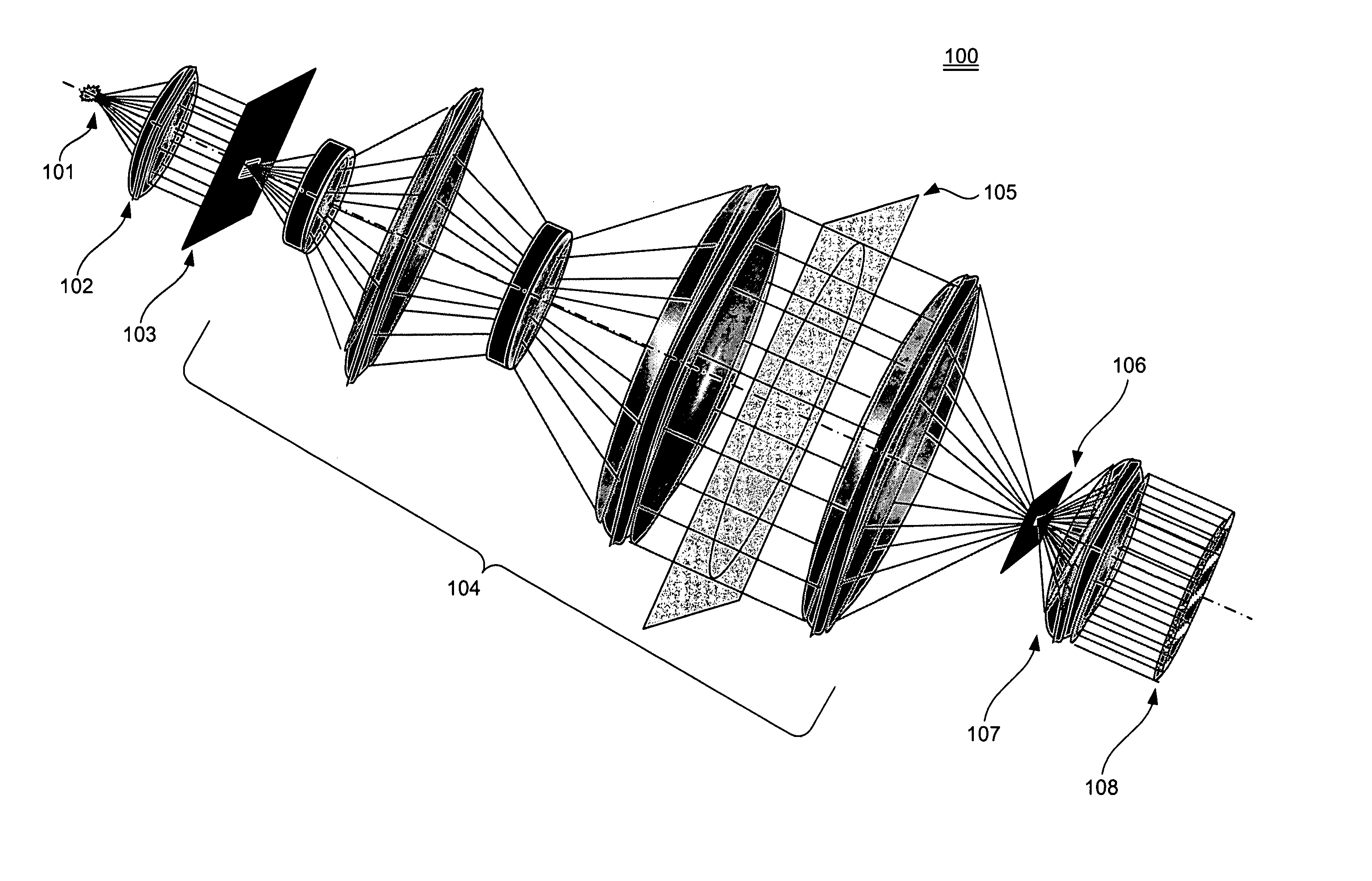
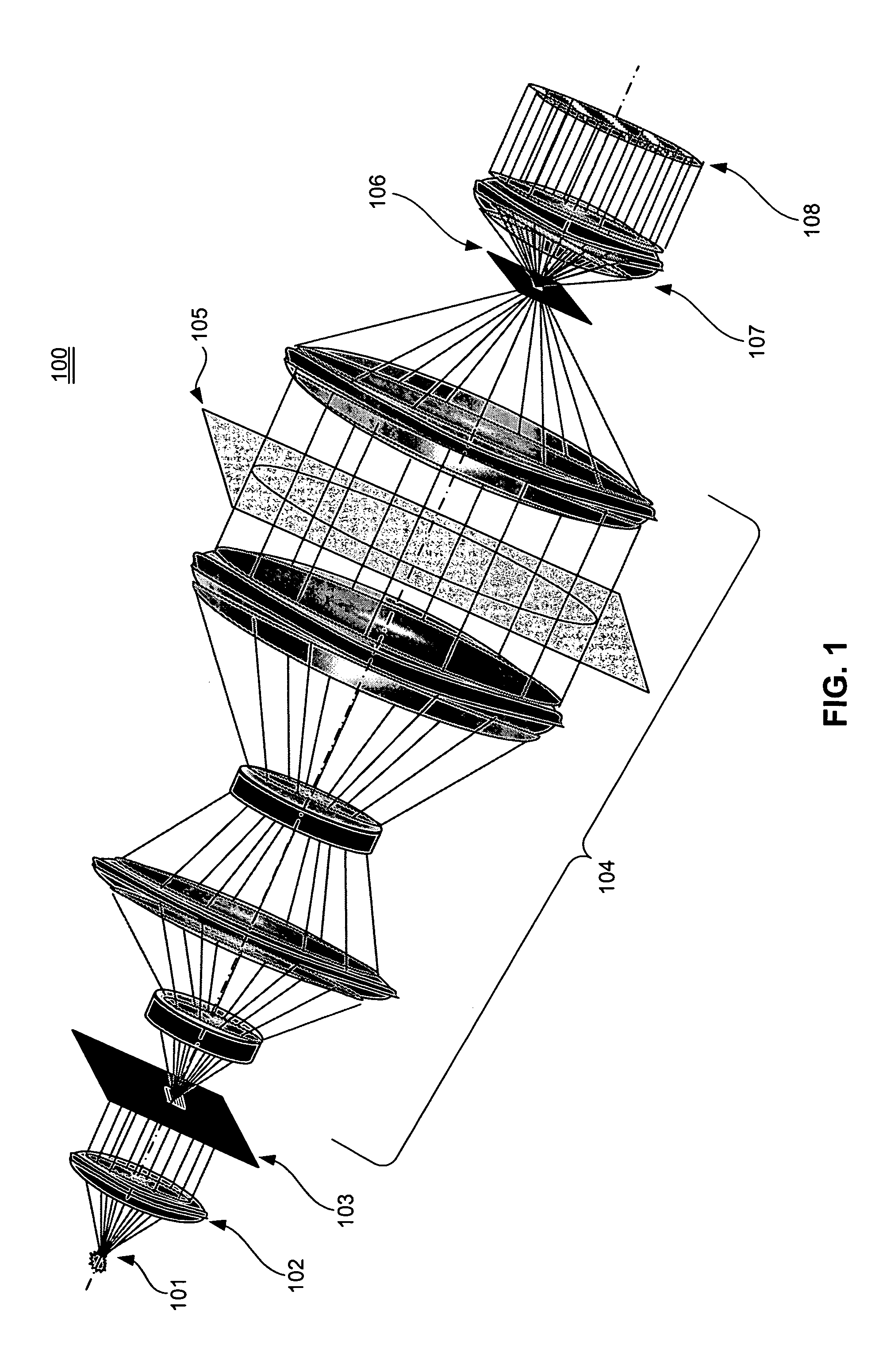
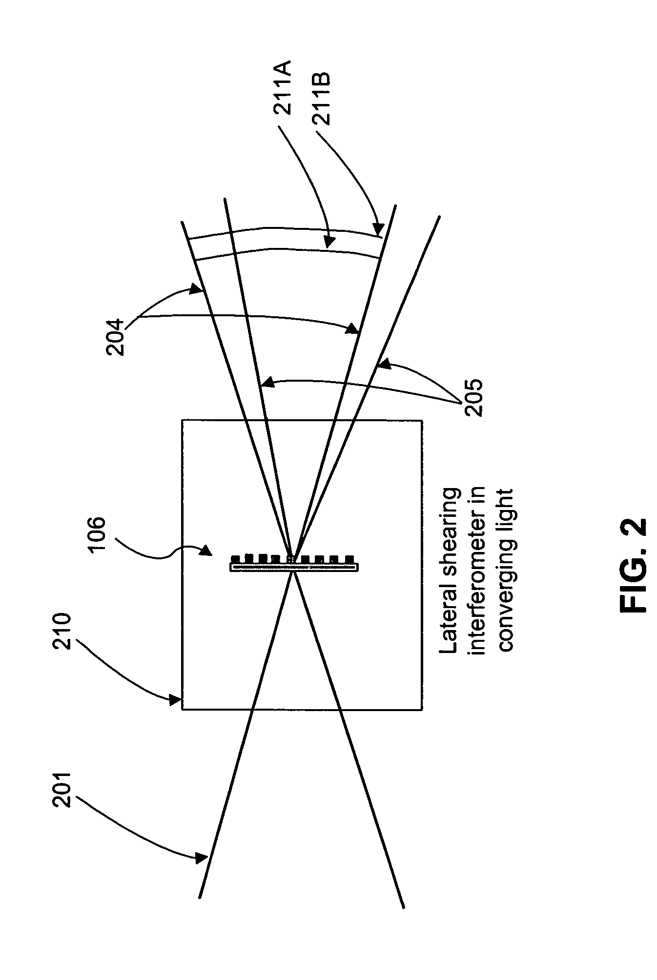
[0025] It is convenient to characterize field-dependent aberrations of a projections optics (PO) by an aberration of a wavefront of a spherical wave emitted from a corresponding field point in the object plane. Various interferometry techniques can be used to measure aberration of this spherical wave. Shearing interferometry based on an extended incoherent source in the object plane superimposed with an object-plane grating matching the shearing grating is described in J. Braat and A. J. E. M. Janssen, Improved Ronchi test with Extended Source, J. Opt. Soc. Am. A, Vol. 16, No. 1, pp. 131-140, January 1999, incorporated by reference herein. Also, the paper by Naulleau et al., Static Microfield Printing at the ALS with the ETS-2 Set Optic, Proc. SPIE 4688, 64-71 (2002) (http: / / goldberg.lbl.gov / papers / Naulleau_SPIE—4688(2002).pdf), inc...
PUM
| Property | Measurement | Unit |
|---|---|---|
| wavelengths | aaaaa | aaaaa |
| wedge angle | aaaaa | aaaaa |
| non-linear phase | aaaaa | aaaaa |
Abstract
Description
Claims
Application Information