DRAM interface circuits having enhanced skew, slew rate and impedance control

a dram interface and impedance control technology, applied in the field of integrated circuit devices, can solve problems such as difficult generation of signals that meet these reduced timing margins, and achieve the effect of enhancing skew, slew rate and output impedance control

Active Publication Date: 2005-11-24
INTEGRATED DEVICE TECH INC
View PDF4 Cites 129 Cited by
  • Summary
  • Abstract
  • Description
  • Claims
  • Application Information

AI Technical Summary

Benefits of technology

[0007] Embodiments of the present invention include a fully-buffered dual in-line memory module (FB-DIMM) with an advanced memory buffer (AMB) having enhanced skew, slew rate and output impedance control. The AMB includes user accessible registers that can be programmed to carefully control the edge placement (or phase) of signals generated from the AMB to multiple DRAMs on the module. This control of edge placement, which may be performed independently for each group of signals: clock (CLK, CLK#), command (RAS, CAS, WE), address (including bank address), data (DQ) and data strobe (DQS), provides 360 degrees of control (or one period). This means that any group of signals can be moved independently by one complete period relatively to any other group. In some embodiments, the skew resolution is 6.5 ps in 384 steps, comprising one full period when the AMB is operating at the 4.8 Gb / s rate.

Problems solved by technology

Generating signals that meet these reduced timing margins is difficult because of the presence of timing skew between data, address, command, strobe and clock signals generated to and from the DRAMs.

Method used


Image

  • DRAM interface circuits having enhanced skew, slew rate and impedance control
  • DRAM interface circuits having enhanced skew, slew rate and impedance control
  • DRAM interface circuits having enhanced skew, slew rate and impedance control

Examples


Embodiment Construction

[0015] The present invention will now be described more fully herein with reference to the accompanying drawings, in which preferred embodiments of the invention are shown. This invention may, however, be embodied in many different forms and should not be construed as being limited to the embodiments set forth herein; rather, these embodiments are provided so that this disclosure will be thorough and complete, and will fully convey the scope of the invention to those skilled in the art. Like reference numerals refer to like elements throughout and signal lines and signals thereon may be referred to by the same reference characters. Signals may also be synchronized and / or undergo minor boolean operations (e.g., inversion) without being considered different signals. The suffix “#” (or prefix symbol “ / ”) to a signal name may also denote a complementary data or information signal or an active low control signal, for example.

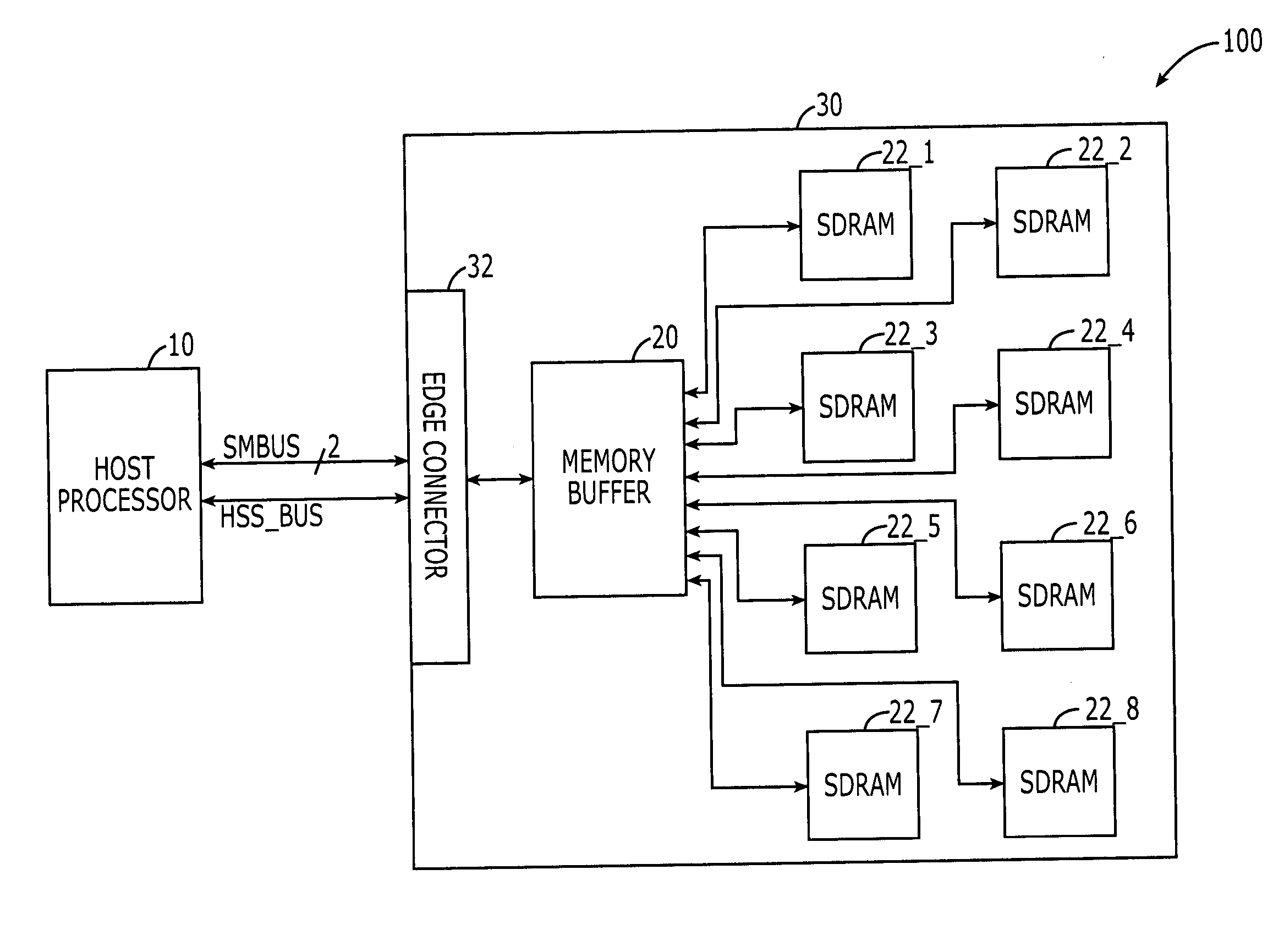
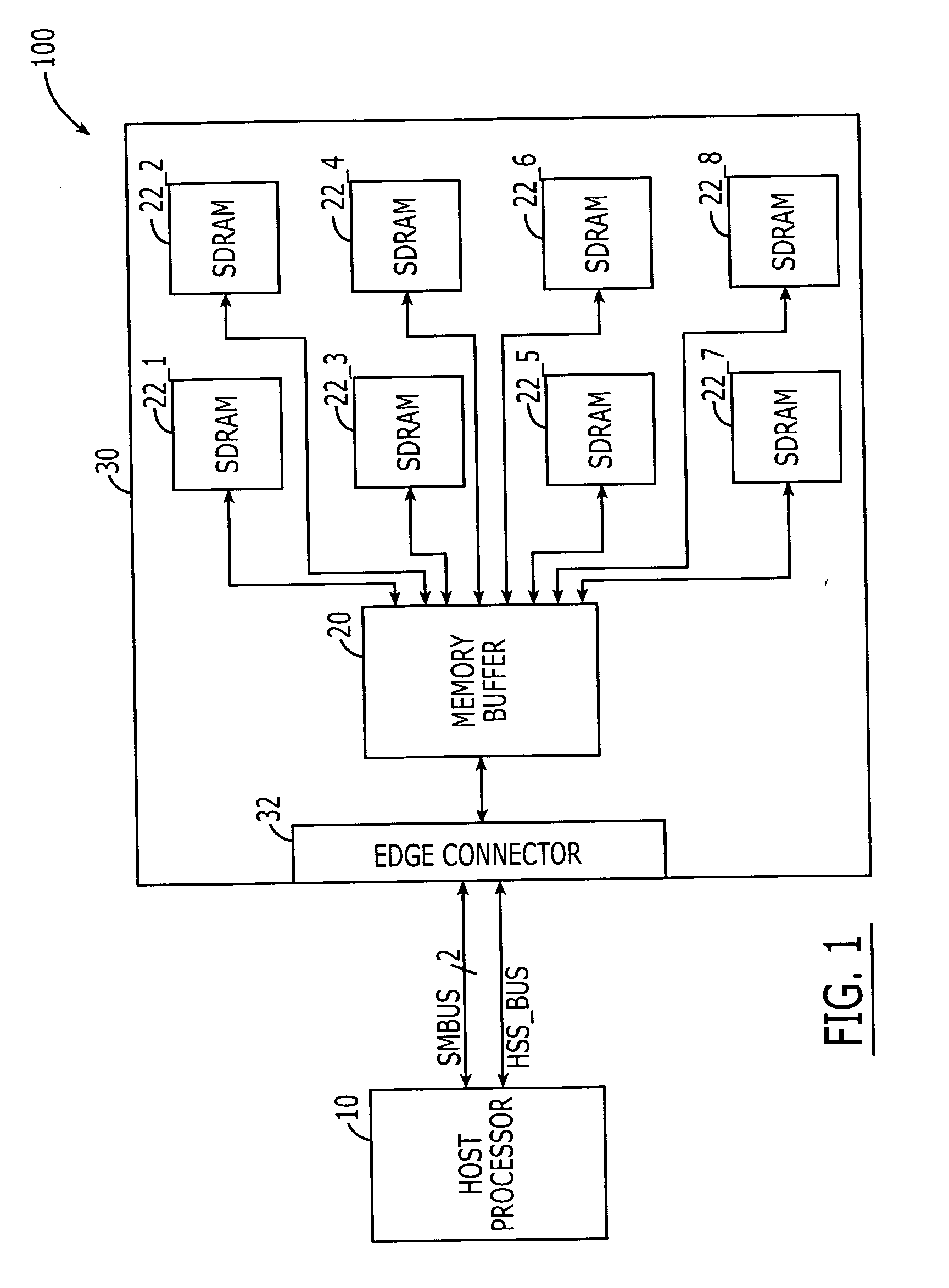
[0016] Referring now to FIG. 1, an integrated circuit system 1...


PUM


Abstract

Fully-buffered dual in-line memory modules (FB-DIMM) include advanced memory buffers (AMBs) having enhanced skew, slew rate and output impedance control. The AMB includes user accessible registers that can be programmed to carefully control the edge placement (or phase) of signals generated from the AMB to multiple DRAMs on the module. This control of edge placement, which may be performed independently for each group of signals: clock (CLK, CLK#), command (RAS, CAS, WE), address (including bank address), data (DQ) and data strobe (DQS), provides 360 degrees of control (or one period). This means that any group of signals can be moved independently by one complete period relatively to any other group.

Description

REFERENCE TO PRIORITY APPLICATION [0001] This application derives priority from U.S. Provisional Application Ser. No. 60 / 573,254, filed May 21, 2004, the disclosure of which is hereby incorporated herein by reference. CROSS-REFERENCE TO RELATED APPLICATIONS [0002] This application discloses subject matter that is related to subject matter disclosed in U.S. application Ser. No. 10 / 643,208, filed Aug. 18, 2003, Ser. No. 10 / 648,090, filed Aug. 26, 2003 and Ser. No. 10 / 616,272, filed Jul. 9, 2003, the disclosures of which are hereby incorporated herein by reference.FIELD OF THE INVENTION [0003] The present invention relates to integrated circuit devices and methods of operating same and, more particularly, to memory devices and methods of operating memory devices. BACKGROUND OF THE INVENTION [0004] A fully-buffered dual in-line memory module (FB-DIMM) may utilize an advanced memory buffer (AMB), which is typically disposed on one side of the module. An AMB may have three ports of commun...

Claims


Application Information

Patent Timeline
Patent Type & Authority Applications(United States)
IPC IPC(8): G11C5/00G11C7/22
CPCG11C7/22
Inventor MURTUGH, PAULKNAACK, ROLAND T.
Owner INTEGRATED DEVICE TECH INC
Why Eureka
Try Eureka