Methods of fabricating a semiconductor device using a dilute aqueous solution of an ammonia and peroxide mixture

a technology of ammonia and peroxide, which is applied in the direction of detergent compositions, crystal growth processes, rotary drilling, etc., can solve the disadvantages of silicon oxide layers being vulnerable, affecting the performance characteristics of the resulting transistor, and causing excessive etching of silicon oxide layers by ammonium hydroxid

Inactive Publication Date: 2005-11-24
SAMSUNG ELECTRONICS CO LTD
View PDF5 Cites 47 Cited by
  • Summary
  • Abstract
  • Description
  • Claims
  • Application Information

AI Technical Summary

Benefits of technology

[0012] According to some embodiments of the present invention, there are provided methods of fabricating a semiconductor device capable of optimizing a physical property of a surface of a (Si1-xGex) alloy layer by using a dilute aqueous solution consisting essentially of an ammonia and peroxide mixture (APM), where “x” is a fraction or a decimal having a value greater than 0 but less than 1.

Problems solved by technology

However, the silicon-germanium layer has the disadvantageous property of being vulnerable to an aqueous solution containing ammonium hydroxide and hydrogen peroxide.
This is because the silicon-germanium layer readily reacts with hydrogen peroxide (H2O2) to first form a silicon oxide layer, and that silicon oxide layer is then excessively etched by the ammonium hydroxide.
Such an excessively etched silicon-germanium layer significantly impairs the performance characteristics of the resulting transistor.
However, the aqueous solution of ammonia and hydrogen peroxide used in this step may excessively etch the upper surface and the sidewalls of the silicon-germanium alloy unless the volume ratios of ammonia and hydrogen peroxide in the aqueous solution are optimized and contact time is carefully controlled.

Method used


Image

  • Methods of fabricating a semiconductor device using a dilute aqueous solution of an ammonia and peroxide mixture
  • Methods of fabricating a semiconductor device using a dilute aqueous solution of an ammonia and peroxide mixture
  • Methods of fabricating a semiconductor device using a dilute aqueous solution of an ammonia and peroxide mixture

Examples


Embodiment Construction

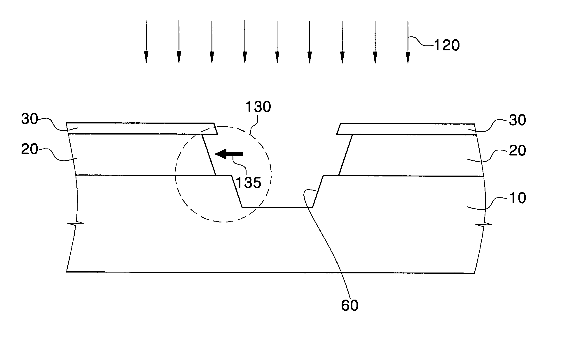
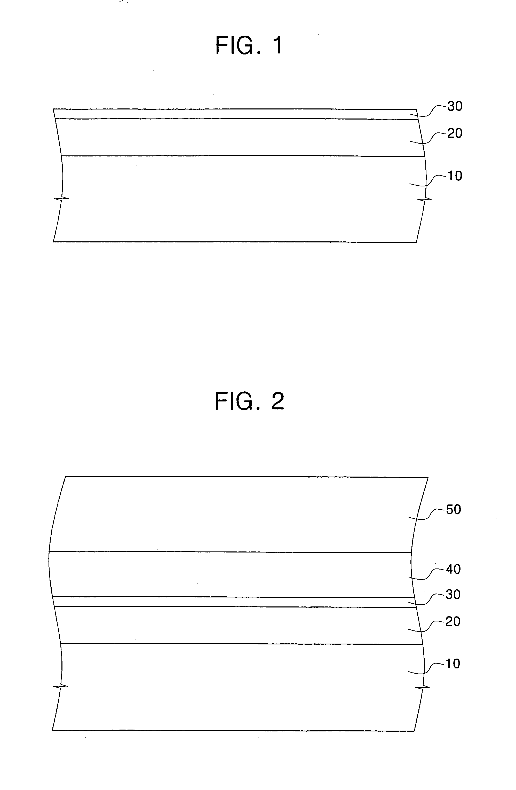
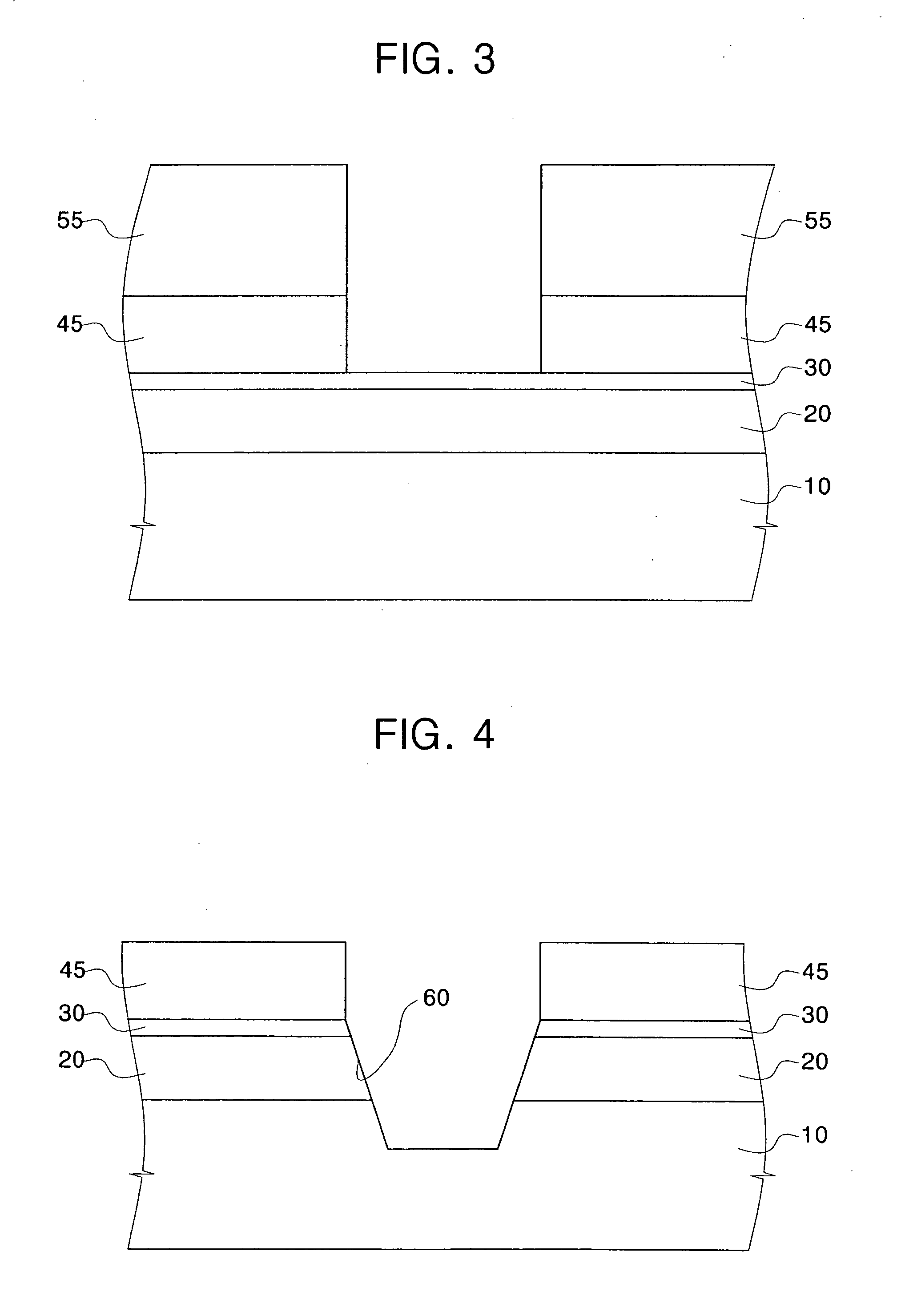
[0021]FIGS. 1 through 5 are schematic cross-sectional views of portions of semiconductor devices illustrating a method of forming a trench in a substrate having a silicon-germanium alloy layer and another material layer according to an embodiment of the invention, respectively.

[0022] Referring to FIGS. 1 through 5, an alloy layer 20 and a material layer 30 are sequentially formed on a suitable semiconductor substrate 10. The material layer 30 may be formed, for example, of a strained silicon layer by using an epitaxial process. The alloy layer 20 is formed of a silicon-germanium (Si1-xGex) alloy layer such that germanium atoms are present in alloy layer 20 in the range of greater than 0 to about 99% by atomic weight with respect to the presence of silicon atoms. The alloy layer 20 having suitable proportions of silicon and germanium may be formed, for example, by using a chemical vapor deposition process. The substrate 10 is preferably formed of a single crystalline silicon layer, ...


PUM

PropertyMeasurementUnit
temperatureaaaaaaaaaa

Abstract

This invention provides methods of fabricating semiconductor devices, wherein an alloy layer is formed on a semiconductor substrate to form a substrate structure, which methods include using an aqueous solution diluted ammonia and peroxide mixture (APM) to perform cleaning and/or wet etching treatment steps on the substrate structure.

Description

CROSS-REFERENCE TO RELATED APPLICATION [0001] This patent application claims priority from Korean Patent Application No. 10-2004-0020521, filed Mar. 25, 2004, the contents of which are hereby incorporated by reference in their entirety. BACKGROUND OF INVENTION [0002] 1. Technical Field [0003] The present invention relates generally to methods of fabricating a semiconductor device, and more particularly, to methods of fabricating a semiconductor device using a dilute aqueous solution of an ammonia and peroxide mixture (hereinafter abbreviated as “APM”). [0004] 2. Discussion of the Related Art [0005] Recently, semiconductor fabrication processes have focused on forming a transistor on a silicon-germanium layer (rather than on a substantially homogeneous single crystalline silicon substrate) in order to meet growing market demand for semiconductor devices having properties of higher speed and a higher degree of integration. The silicon-germanium layer is typically formed by appling ger...

Claims


Application Information

Patent Timeline
Patent Type & Authority Applications(United States)
IPC IPC(8): C30B1/00H01L21/00H01L21/20H01L21/306H01L21/304H01L21/36
CPCH01L21/02052E21B3/045
Inventor KWON, DOO-WONKO, HYUNG-HOMUN, CHANG-SUPSHIM, WOO-GWANPARK, IM-SOOKIM, YU-KYUNGHAN, JEONG-NAM
Owner SAMSUNG ELECTRONICS CO LTD
Why Eureka
Try Eureka