Method for manufacturing graphene, transparent electrode and active layer comprising the same, and display, electronic device, optoelectronic device, battery, solar cell, and dye-sensitized solar cell including the electrode and the active layer

A transparent electrode, graphene technology, applied in the production of graphene, transparent electrodes and active layers comprising graphene, and displays, electronic devices, optoelectronic devices, batteries, solar cells and In the field of dye-sensitized solar cells, it can solve the problems of uneven threshold voltage and leakage current, and achieve the effect of excellent physical and electrical properties.

Inactive Publication Date: 2012-11-21
UNIST (ULSAN NAT INST OF SCI & TECH)
View PDF3 Cites 21 Cited by
  • Summary
  • Abstract
  • Description
  • Claims
  • Application Information

AI Technical Summary

Problems solved by technology

[0011] Polysilicon can be used as a semiconductor layer to provide high mobility, but the threshold voltage of TFT may not be uniform
[0012] In addition, leakage current may occur in the amorphous silicon or polysilicon layer when light such as light from a backlight unit is incident thereon

Method used


Image

  • Method for manufacturing graphene, transparent electrode and active layer comprising the same, and display, electronic device, optoelectronic device, battery, solar cell, and dye-sensitized solar cell including the electrode and the active layer
  • Method for manufacturing graphene, transparent electrode and active layer comprising the same, and display, electronic device, optoelectronic device, battery, solar cell, and dye-sensitized solar cell including the electrode and the active layer
  • Method for manufacturing graphene, transparent electrode and active layer comprising the same, and display, electronic device, optoelectronic device, battery, solar cell, and dye-sensitized solar cell including the electrode and the active layer

Examples


Embodiment 1

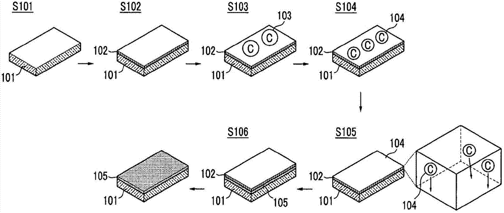
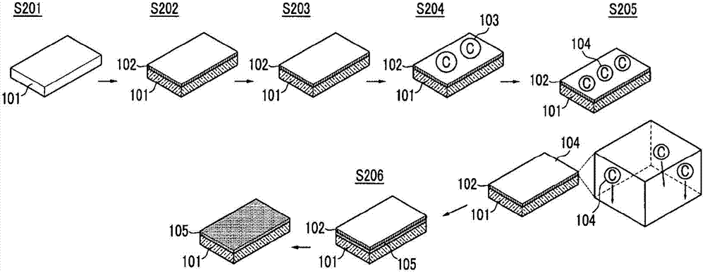
[0177] Example 1: Graphene grows directly on SiO 2 / Si substrate

[0178] A liquid carbon source material according to one embodiment of the present invention is used to directly grow on SiO 2 / Si substrate. SiO 2 is a 300nm thick layer and is deposited on a Si substrate by conventional thermal growth methods.

[0179] Clean SiO 2 / Si substrate surface. Then, a 100 nm thick Ni film was deposited on SiO using an electron beam evaporator 2 / Si substrate. During nickel deposition the SiO 2 / Si substrate maintained at 400°C.

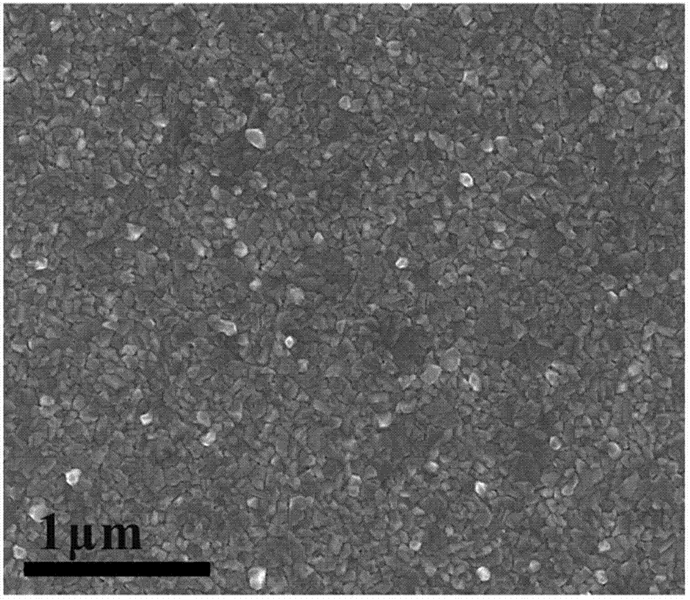
[0180] image 3 SEM images of the deposited nickel films are provided.

[0181] SEM images show that the nickel thin film is polycrystalline. It has grains with an average size of about 100 nm.

[0182] The nickel thin film is heat treated to improve orientation and increase average grain size. Heat treatment is carried out in a high vacuum chamber. The chamber was subjected to a hydrogen atmosphere using high purity (99.9999%) hydrogen. ...

Embodiment 2

[0190] Graphene was formed according to the same method as in Example 1, except that the heating temperature after placing the carbon source material on the nickel thin film was 160°C.

[0191] Figure 6 SEM images of graphene according to Example 2 are provided.

[0192] Such as Figure 6 As shown, the graphene according to Example 2 has large grains with an average size ranging from several micrometers to tens of micrometers. The SEM images show clear brightness contrasts that depend on thickness. The brightest image indicates single-layer graphene C, the brightest image indicates bilayer graphene B, and the darkest image indicates multilayer graphene A.

[0193] In addition, if Figure 6 As shown, the graphene according to Example 2 is formed at low temperature and thus has no wrinkles due to the difference in thermal expansion coefficient between the graphene and the underlying substrate. In general, wrinkles may degrade the physical properties of graphene.

Embodiment 3

[0195] Graphene was formed according to the same method as in Example 1, except that the heating temperature and time after placing the carbon source material on the nickel thin film were 60° C. and 10 minutes, respectively.


PUM

PropertyMeasurementUnit
thicknessaaaaaaaaaa
thicknessaaaaaaaaaa
sizeaaaaaaaaaa

Abstract

Disclosed is a method of manufacturing graphene, a transparent electrode and an active layer including the graphene, and a display, an electronic device, an optoelectronic device, a solar cell, and a dye-sensitized solar cell including the transparent electrode and the active layer. The method of manufacturing graphene includes: (a) preparing a subject substrate; (b) forming a metal thin film on the subject substrate and heat-treating the metal thin film to increase the grain size of the metal thin film; (c) supplying a carbon source material on the metal thin film; (d) heating the supplied carbon source material, the subject substrate, and the metal thin film; (e) diffusing carbon atoms generated from the heated carbon source material due to thermal decomposition into the metal thin film; and (f) forming graphene on the subject substrate by the carbon atoms diffused through the metal thin film.

Description

[0001] Cross References to Related Applications [0002] This application claims priority to Korean Patent Application No. 10-2010-0020990 filed on Mar. 9, 2010 at the Korean Intellectual Property Office and Korean Patent Application No. 10-2010-0126995 filed on Dec. 13, 2010 at the Korean Intellectual Property Office rights and interests, the entire contents of which are hereby incorporated by reference. Background of the invention [0003] (a) Field of Invention [0004] The present invention relates to methods for producing graphene, transparent electrodes and active layers comprising graphene, and displays, electronic devices, optoelectronic devices, batteries, solar cells and dye-sensitized solar cells comprising said transparent electrodes and / or said active layers Battery. [0005] (b) Description of relevant fields [0006] In general, because various devices such as displays, LEDs, etc. transmit light to display images or generate electricity, they necessarily requ...

Claims


Application Information

Patent Timeline
Patent Type & Authority Applications(China)
IPC IPC(8): C01B31/02H01B1/04G02F1/1343H01L31/042
CPCY02E60/12H01M4/587C01B31/0453B82Y30/00G02F1/155H01L31/022466H01L31/1884G02F1/15B82Y40/00H01M4/663H01B1/04Y02E10/50C01B31/0446H01L51/442Y02E10/542C01B32/184Y02E10/549Y02P70/50Y02E60/10H10K30/82C01B32/186
Inventor 权纯瑢朴基馥尹义埈郭珍诚
Owner UNIST (ULSAN NAT INST OF SCI & TECH)
Why Eureka
Try Eureka