Semiconductor device

a technology of mmic and fets, applied in the field of mmiconductor devices, can solve the problems of increased insertion loss, inability to observe and inability to detect the addition of insertion loss

Active Publication Date: 2005-12-01
SEMICON COMPONENTS IND LLC
View PDF19 Cites 12 Cited by
  • Summary
  • Abstract
  • Description
  • Claims
  • Application Information

AI Technical Summary

Benefits of technology

[0024] The present invention also provides a semiconductor device that includes a compound semiconductor substrate; a first conducting region disposed in or on the substrate; a first metal layer configured to receive a first predetermined electric potential and connected with the first conducting region; a second conducting region disposed in or on the substrate; a second metal layer configured to receive a second predetermined electric potential and connected with the second conducting region; and a floating conducting region disposed in or on the substrate, the floating conducting region being configured not to receive any electric potential and disposed between the first and second conducting regions.
[0024] The present invention also provides a semiconductor device that includes a compound semiconductor substrate; a first conducting region disposed in or on the substrate; a first metal layer configured to receive a first predetermined electric potential and connected with the first conducting region; a second conducting region disposed in or on the substrate; a second metal layer configured to receive a second predetermined electric potential and connected with the second conducting region; and a floating conducting region disposed in or on the substrate, the floating conducting region being configured not to receive any electric potential and disposed between the first and second conducting regions.
[0024] The present invention also provides a semiconductor device that includes a compound semiconductor substrate; a first conducting region disposed in or on the substrate; a first metal layer configured to receive a first predetermined electric potential and connected with the first conducting region; a second conducting region disposed in or on the substrate; a second metal layer configured to receive a second predetermined electric potential and connected with the second conducting region; and a floating conducting region disposed in or on the substrate, the floating conducting region being configured not to receive any electric potential and disposed between the first and second conducting regions.
[0018] Thus, the resistors R1 and R2 can be placed in parallel between the common input terminal pad I and the FETs. Additionally, the resistors R1 and R2 and the common input terminal pad I can be closely placed at a distance of 4 μm from each other. Accordingly, an enlargement of the chip can be suppressed even if the chip has a reverse control pattern.
[0129] Fifth, one part of adjacent ones of the conducting regions to which predetermined potentials are applied is placed under a common input terminal pad or around the pad, and another part thereof is a connection connected to a control terminal pad. It is possible to effectively prevent the leakage of high-frequency signals between the common input terminal pad to which a high-frequency signal is inputted and the control terminal pad which is at GND potential at high frequencies. Consequently, an increase in insertion loss can be suppressed.
[0130] Sixth, at least part of the connection is a resistor, and the leakage of high-frequency signals can be prevented using the conducting region at a floating potential. Accordingly, the common input terminal pad and the resistor connected to the control terminal pad can be closely placed. This makes it possible to effectively prevent the leakage of high-frequency signals in a reverse control pattern in which resistors are lied around long distance in a chip.
[0131] Seventh, at least one part of the conducting regions to which predetermined potentials are applied is the operating region of an FET. Accordingly, it is possible to prevent the leakage of high-frequency signals caused by a depletion layer extending from the FET to the substrate.
[0018] Thus, the resistors R1 and R2 can be placed in parallel between the common input terminal pad I and the FETs. Additionally, the resistors R1 and R2 and the common input terminal pad I can be closely placed at a distance of 4 μm from each other. Accordingly, an enlargement of the chip can be suppressed even if the chip has a reverse control pattern.
[0133] Ninth, the FETs are HEMTs having small insertion losses of basic devices themselves, and an MMIC can be formed in which low insertion loss characteristics of HEMTs are sufficiently utilized by preventing even a small leakage of high-frequency signals in a pattern shape.
[0047] Further, in order to suppress the spread of a depletion layer extending from each of the pads(I,O1,O2,C1 and C2) to the substrate and hence improve isolation, a peripheral impurity region 100a which is a heavily-doped impurity region is placed around each of the pads. Furthermore, the peripheral impurity region 100a is also placed around each of the gate wirings 27, where the peripheral impurity region 100a is electrically connected to the gate wiring 27.

Problems solved by technology

However, when a switch circuit device was constructed in the same pattern as that of the above-described one using HEMTs instead of the GaAs FETs, it was revealed that insertion loss increased, which is loss in the transmission of a high-frequency signal from the common input terminal IN to the output terminal OUT1.
The MMIC using GaAs FETs also potentially has an addition of insertion loss due to the aforementioned pattern shape by an amount similar to that in the MMIC using HEMTs.
However, the addition of insertion loss was not observed, because the insertion loss of a GaAs FET itself is large and the proportion of the addition of insertion loss is negligible.

Method used


Image

  • Semiconductor device
  • Semiconductor device
  • Semiconductor device

Examples


first embodiment

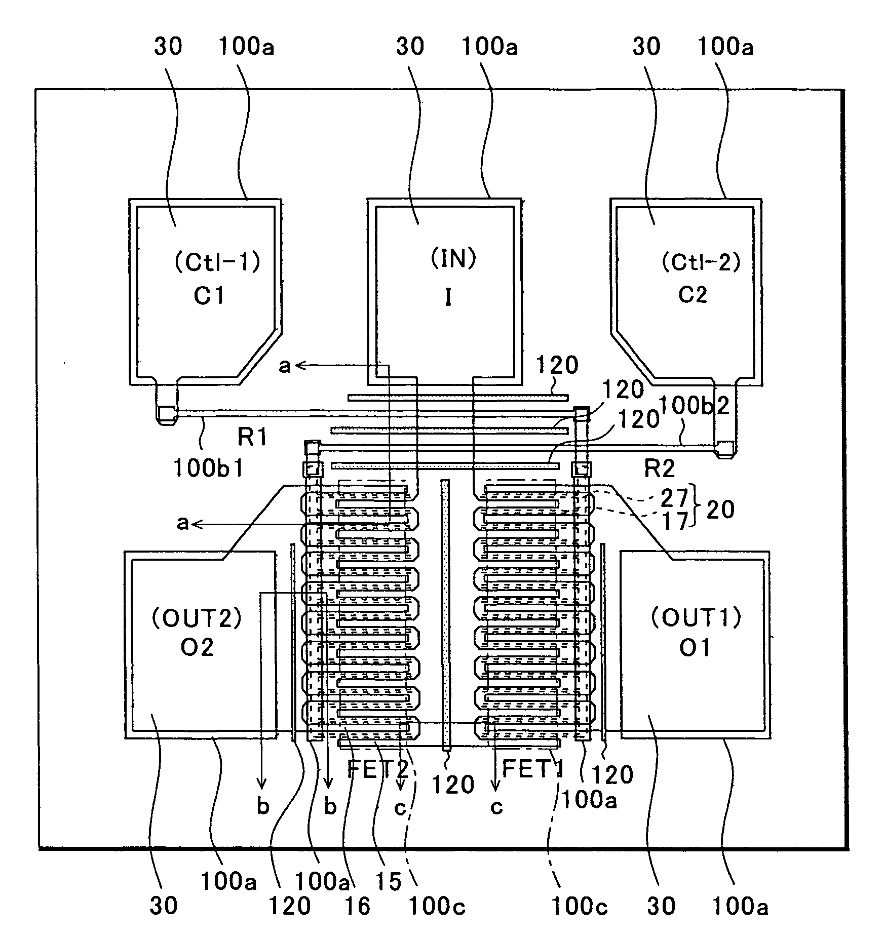
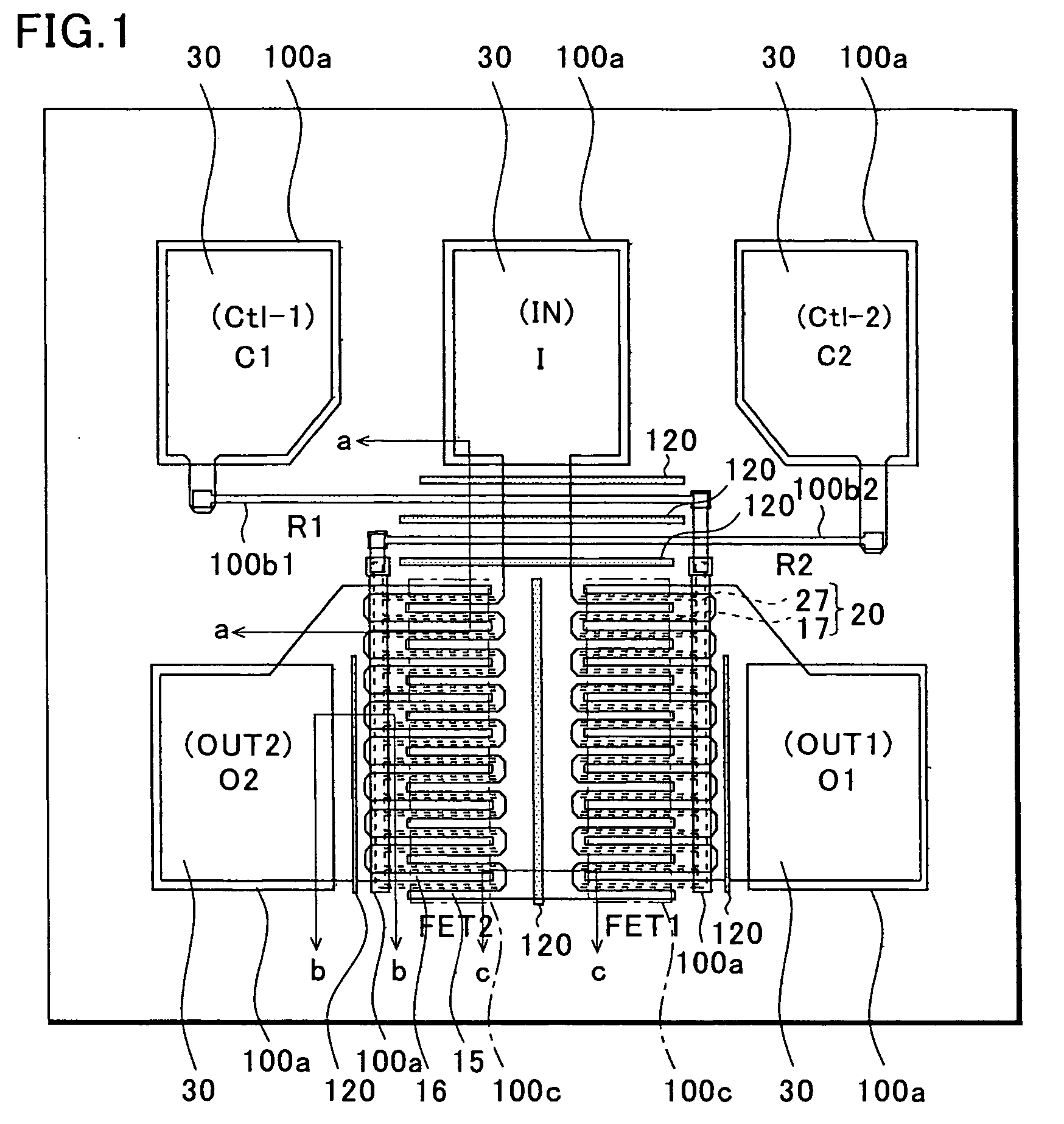
[0038] First, using FIGS. 1 to 2C, the present invention will be described by taking as an example an SPDT switch circuit device using GaAs MESFETs.

[0039]FIG. 1 is a plan view showing the first embodiment. The circuit diagram thereof is the same as that of FIG. 10B, and therefore omitted. The source electrodes (or drain electrodes) of first and second FETs FET1 and FET2 are connected to a common input terminal IN. The gate electrodes of the FET1 and FET2 are connected to first and second control terminals Ctl-1 and Ctl-2 through resistors R1 and R2, respectively. Further, the drain electrodes (or source electrodes) of the FET1 and FET2 are connected to first and second output terminals OUT1 and OUT2, respectively. Control signals which are applied to the first and second control terminals Ctl-1 and Ctl-2 are complementary signals. Of the FET1 and FET2, one to which an H-level signal is applied is turned on, whereby an input high-frequency signal entering the common input terminal IN...

second embodiment

[0064] Next, the present invention will be described with reference to FIG. 3.

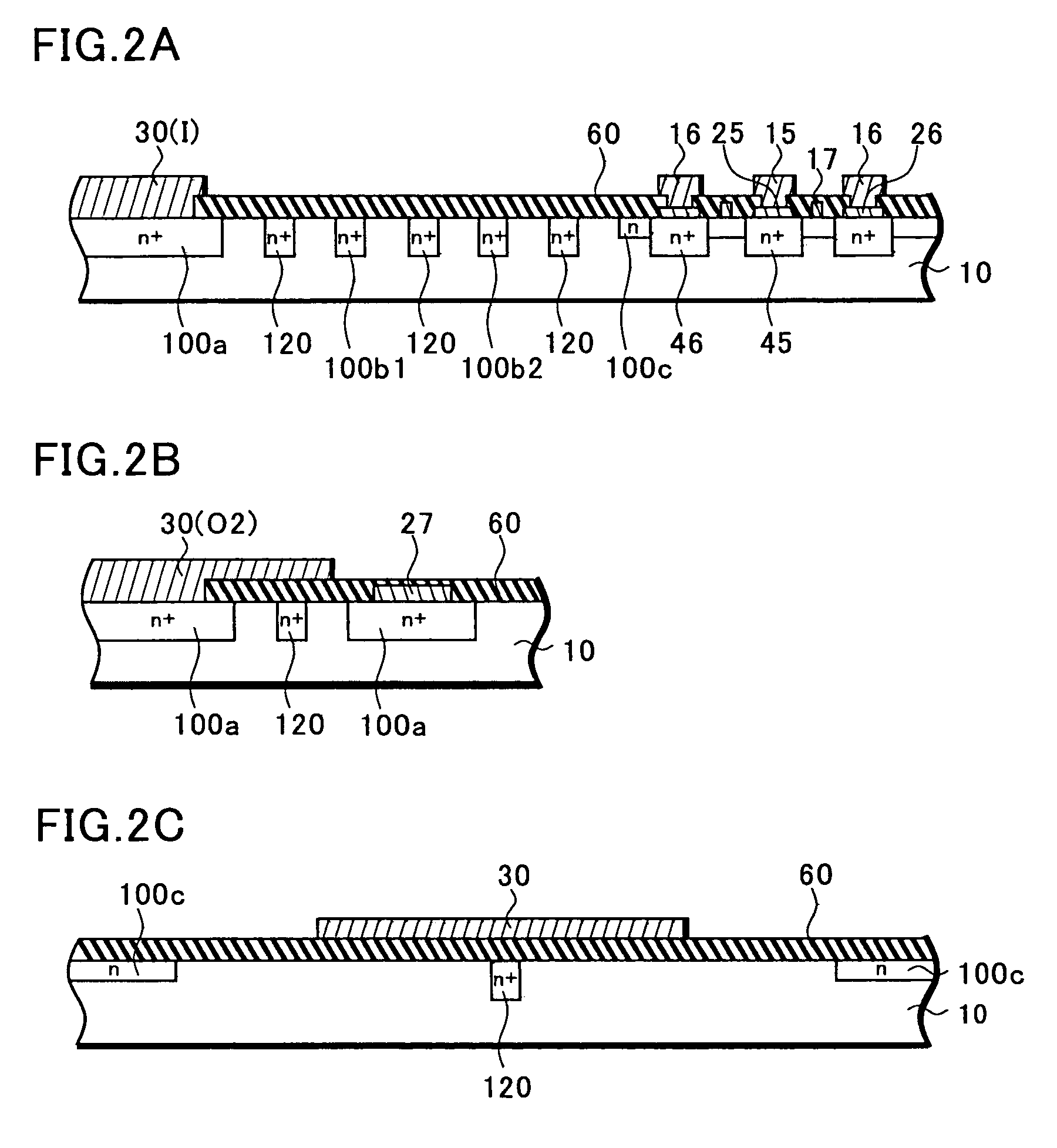
[0065] The second embodiment is the case where basic devices are HEMTs, and is provided with a pattern similar to that for the case of GaAs FETs shown in the first embodiment. That is, a plan view thereof is similar to that of FIG. 1 and therefore will not be described. A description will be given with reference to the cross-sectional views of FIGS. 3A to 3C. Note that FIG. 3A is a cross-sectional view taken along the a-a line of FIG. 1, FIG. 3B is a cross-sectional view taken along the b-b line of FIG. 1, and FIG. 3C is a cross-sectional view taken along the c-c line of FIG. 1.

[0066] In a HEMT, an undoped buffer layer 32 is deposited on a semi-insulating GaAs substrate 31. In most of the relevant cases, the buffer layer is formed of a plurality of layers. Further, an n+ type AlGaAs layer 33 to serve as an electron-supplying layer, an undoped InGaAs layer 35 to serve as a channel (electron transit) layer,...

fourth embodiment

[0108] Furthermore, a fourth embodiment will be described with reference to FIGS. 8 and 9.

[0109] The fourth embodiment is a switch circuit device for high-power application in which a plurality of stages of FETs are connected in series.

[0110]FIG. 8 is a circuit diagram showing one example of a multistage-connection compound semiconductor switch circuit device. This switch circuit device is also an SPDT switch. There are five external terminals: a common input terminal IN, first and second output terminals OUT1 and OUT2, and first and second control terminals Ctl-1 and Ctl-2.

[0111] As shown in FIG. 8, the switch circuit device includes first and second FET groups F1 and F2, each of which has, for example, two stages of FETs connected in series. Further, a source electrode (or a drain electrode) of an FET FET1-1 of the first FET group F1 and a source electrode (or a drain electrode) of an FET FET2-1 of the second FET group F2 are connected to the common input terminal IN. The gate e...


PUM


Abstract

Floating conducting regions at floating potentials are placed on a substrate surface between adjacent conducting regions to which predetermined potentials are applied. This makes it possible to block the spread of a depletion layer to the substrate between the conducting impurity regions. Thus, the leakage of high-frequency signals can be suppressed. In particular, in a case where a floating conducting region is placed between a peripheral impurity region of a common input terminal pad and a resistor in a switch circuit device, it is possible to suppress the leakage of high-frequency signals from an input terminal to control terminals which become high frequency GND and to suppress an increase in insertion loss.

Description

BACKGROUND OF THE INVENTION [0001] 1. Field of the Invention [0002] The present invention relates to a semiconductor device. In particular, the present invention relates to a semiconductor device in which insertion loss is reduced. [0003] 2. Description of the Related Art [0004] In mobile communication devices including mobile phones, microwaves in the GHz band are often used, and switch elements for switching high-frequency signals are often used for antenna switch circuits and transmitting / receiving switch circuits (e.g., Japanese Patent Application Publication No. Hei 9(1997)-181642). Since such elements deal with high frequencies, field effect transistors (hereinafter referred to as FETs) using gallium arsenide (GaAs) are often used as such elements. Along with this, monolithic microwave integrated circuits (MMICs) are being developed into which a switch circuit itself, such as described above, is integrated. [0005]FIGS. 10A and 10B show circuit diagrams of compound semiconducto...

Claims


Application Information

Patent Timeline
Patent Type & Authority Applications(United States)
IPC IPC(8): H01L21/338H01L27/095H01L23/34H01L29/778H01L29/812H03K17/00H03K17/693
CPCH01L29/7785H01L29/812H03K17/693H01L2924/0002H01L2924/00H01L27/04H03K17/00
Inventor ASANO, TETSURO
Owner SEMICON COMPONENTS IND LLC
Why Eureka
Try Eureka