Organic electroluminescent device and method for manufacturing the same

a light-emitting diode and organic technology, applied in the direction of luminescnet screens, discharge tubes, identification means, etc., can solve the problems of inability to improve resolution ability, inability to achieve, and easy to affect each other, so as to improve light-emitting efficiency, enhance grayscale and contrast effect, and reduce interference of external light sources

Inactive Publication Date: 2005-12-01
UNIVISION TECHNOLOGY
View PDF0 Cites 12 Cited by
  • Summary
  • Abstract
  • Description
  • Claims
  • Application Information

AI Technical Summary

Benefits of technology

[0006] It is a primary object of the present invention to provide an organic light emitting diode element and a manufacturing method thereof which can have light emitting area with bounded pixels and reduce interference of external light source to improve light emitting efficiency, enhance grayscale and contrast effect to improve resolution ability and avoid from additional cost of adding a polarizer.
[0008] To achieve the previous mentioned object, the present invention provides a method of manufacturing an organic electroluminescent device comprises: (a) placing a substrate and growing a black matrix film; (b) making a black matrix pattern by a lithographic etching process; (c) growing a passivation layer on the structure; (d) growing an anode film on the passivation layer; (e) making an anode pattern by a lithographic etching process; (f) coating a photoresist material and making an isolation area by a lithography process; and (g) making a luminescent layer structure. The black matrix pattern is used to bound light emitting area of pixels to reduce the interference of external light source and improve resolution ability.

Problems solved by technology

However, in the prior art technology, when light emitted from different EML or external light enters the prior art organic light emitting diode element 10, it is easily affected each other.
The resolution ability cannot be improved, and an effect of having light emitting area with bounded pixels and reducing mutual interference between EML with different colors at the same time cannot be achieved.

Method used


Image

  • Organic electroluminescent device and method for manufacturing the same
  • Organic electroluminescent device and method for manufacturing the same
  • Organic electroluminescent device and method for manufacturing the same

Examples


first embodiment

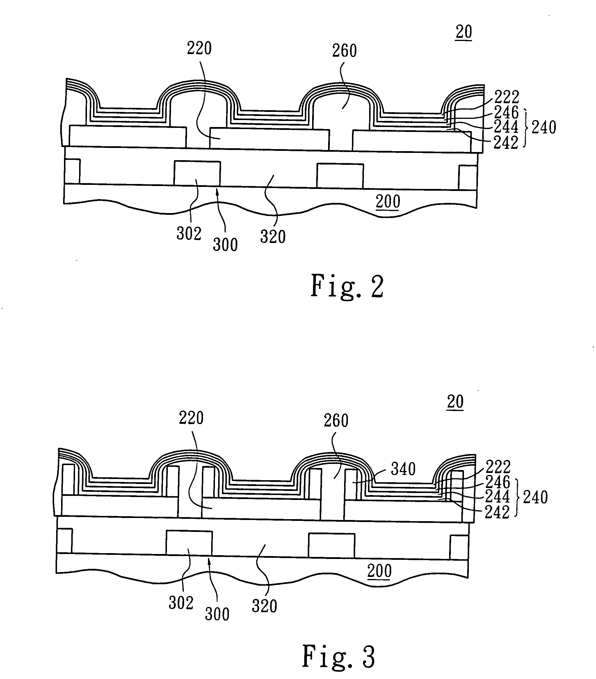
[0022] Please refer to FIG. 2, an organic light emitting diode (OLED) element 20 of the present invention which comprises a substrate 200, a black matrix pattern layer 300 deposited on the substrate 200 as a predetermined pattern, a protection layer 320 laying over on the substrate 200 and the black matrix pattern layer 300, an anode pattern layer 220 deposited on the passivation layer 320 as a predetermined pattern, a luminescent layer structure 240 deposited on the anode pattern layer 220, and an isolation area 260 being between the anode pattern layer 220 as an isolation. Among them, the black matrix pattern layer 300 has low reflectivity, and the black matrix pattern layer 300 has a first matrix pattern 302 corresponding to the isolation area 260. Among them, the luminescent layer structure 240 comprises HTL 242, EML 244, and ETL 246 in an order from bottom to top. After the current is passed into the anode pattern layer 220 and the cathode layer 222, the electronic hole combine...

second embodiment

[0025] Please refer to FIG. 3 and FIG. 4, the present invention. The organic light emitting diode element 20 further comprises a metallic matrix pattern 340 deposited around the anode pattern layer 220. Therefore, the metallic matrix pattern 340 distributed around the pixels can be used to define light emitting area of visible pixels. According to the embodiment, light with different EL colors can be avoided from interfering with each other, and further external light can be avoided from entering into the organic plane light emitting display. As shown in FIG. 3, the metallic matrix pattern 340 is on the edge of the anode pattern layer 220; the metallic matrix pattern 340 is at the side edge (not shown) of the anode pattern layer 220; or the metallic matrix pattern 340 is at the edge of the anode pattern layer 220 and covers the upper edge and side edge (please refer to FIG. 5) of the anode pattern layer 220. The metallic matrix pattern can be made from a material with high conductiv...

third embodiment

[0028] Please refer to FIG. 11A to FIG. 11I, manufacturing flow charts in accordance with the present invention which comprises the following steps: (a) placing a substrate 200 and using chemical, such as detergent, and deionized water to wash the substrate 200, and then using sputter machine to grow a black matrix film 300, such as chromium oxide; (b) making the black matrix pattern 300 by a lithographic etching process; (c) coating polyimide or acrylic on the structure, and then growing a passivation layer 320, such as silicon oxide or silicon oxide nitride membrane, by a chemical vapor deposit (CVD) process; (d) growing ITO membrane 220 to be an anode on the passivation layer 320; (e) making the anode pattern 220 by a lithographic etching process; 9f) using a sputter or electroplating machine to grow a metallic film 340; (g) making the metallic matrix pattern 340 by a lithographic etching process; (h) coating photoresist material and making an isolation area 260 by lithography pr...


PUM


Abstract

An organic electroluminescent device comprises a substrate; a black matrix pattern layer deposited on the substrate as a predetermined pattern; a passivation layer laying over the substrate and the black matrix pattern layer; an anode pattern layer deposited on the passivation as a predetermined pattern; a luminescent layer structure deposited on the anode pattern layer; and an isolation area being an isolation between the anode pattern layer. Among them, the black matrix pattern layer has low reflectivity, and the black matrix pattern layer has a first matrix pattern corresponding to the isolation area or further comprises a second matrix pattern corresponding to the anode pattern layer.

Description

FIELD OF THE INVENTION [0001] The present invention is related to an organic light emitting diode, and more particularly to an organic light emitting diode with light emitting area with bounded pixels and improved light emitting efficiency and enhanced light source contrast effect. BACKGROUND [0002] Please refer to FIG. 1, a cross section view of a prior art organic light emitting diode element 10. The organic light emitting diode element 10 mainly comprises a substrate 100, an anode pattern layer 120 formed a predetermined pattern on the substrate 100, a luminescent layer structure 140 mainly on the anode pattern layer 120, a cathode layer 122 on the luminescent layer structure 140, and an isolation area 160 in the anode pattern layer 120 as an isolation. Among them, the luminescent layer structure 140 comprises HTL 142, EML 144, and ETL 146 in an order from bottom to top. After the current is passed through the anode pattern layer 120 and the cathode layer 122, electronic hole com...

Claims


Application Information

Patent Timeline
Patent Type & Authority Applications(United States)
IPC IPC(8): G09F9/30H01L27/32H05B33/22H01L51/50H01L51/52H05B33/00H05B33/10H05B33/12H05B33/14
CPCH01L51/5284H10K50/865H05B33/22H05B33/10
Inventor LAN, WEN-JENGCHANG CHIEN, CHIN CHUNGYU, HUI CHANG
Owner UNIVISION TECHNOLOGY
Why Eureka
Try Eureka