Chip-type electronic component

a chip-type electronic component and chip-type technology, applied in the direction of resistor housing/enclosement/embedding, fixed capacitor details, fixed capacitors, etc., can solve the problems of low mechanical strength of the miniaturized chip-type electronic component itself, difficult to make visible the information on the component surface, and complicated operation during mounting and repair. , to achieve the effect of high mechanical strength, high visibility of information, and preventing loss

Active Publication Date: 2005-12-01
KYOCERA CORP
View PDF6 Cites 28 Cited by
  • Summary
  • Abstract
  • Description
  • Claims
  • Application Information

AI Technical Summary

Benefits of technology

[0011] A main advantage of the present invention is to provide a chip-type electronic component, though it is small, that exhibits a high visibility of information described on the component surface at the time of mounting.
[0012] Other advantage of the present invention is to provide a chip-type electronic component, though it is small, that has a high mechanical strength.
[0013] Still other advantage of the present invention is to provide a chip-type electronic component that can prevent loss such as chipping, though it is small.
[0014] Still other advantage of the present invention is to provide a chip-type electronic component, though it is small, that can prevent breakage of an external electrode by thickening the external electrode, and that can enlarge a ceramic body.
[0015] To achieve the above advantages, a chip-type electronic component of the present invention comprises a ceramic body having at its interior a conductor pa

Problems solved by technology

Since there are a large variety of chips on the substrate as above described, the operations during mounting and repair are complicated.
However, due to the high densification of the substrate and the miniaturization of the chip-type electronic component, it is difficult to make visible the information on the component surface.
Moreover, the miniaturized chip-type electronic component itself is of low mechanical strength.
Therefore, there arises the problem that, when the chip-type electronic component is transported and mounted onto the substrate by an automatic machine, it may be broken depending on the grip strength, and the speed and strength when it is disposed on the

Method used


Image

  • Chip-type electronic component
  • Chip-type electronic component
  • Chip-type electronic component

Examples


first preferred embodiment

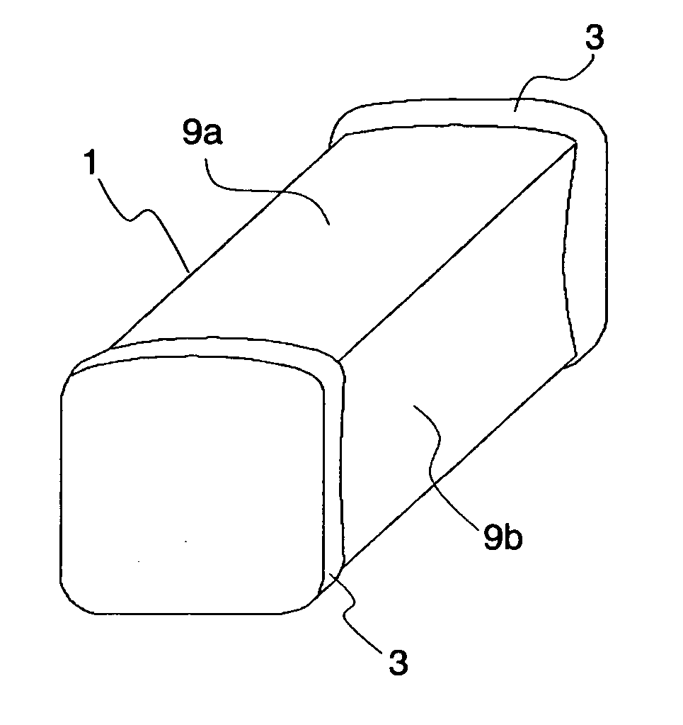
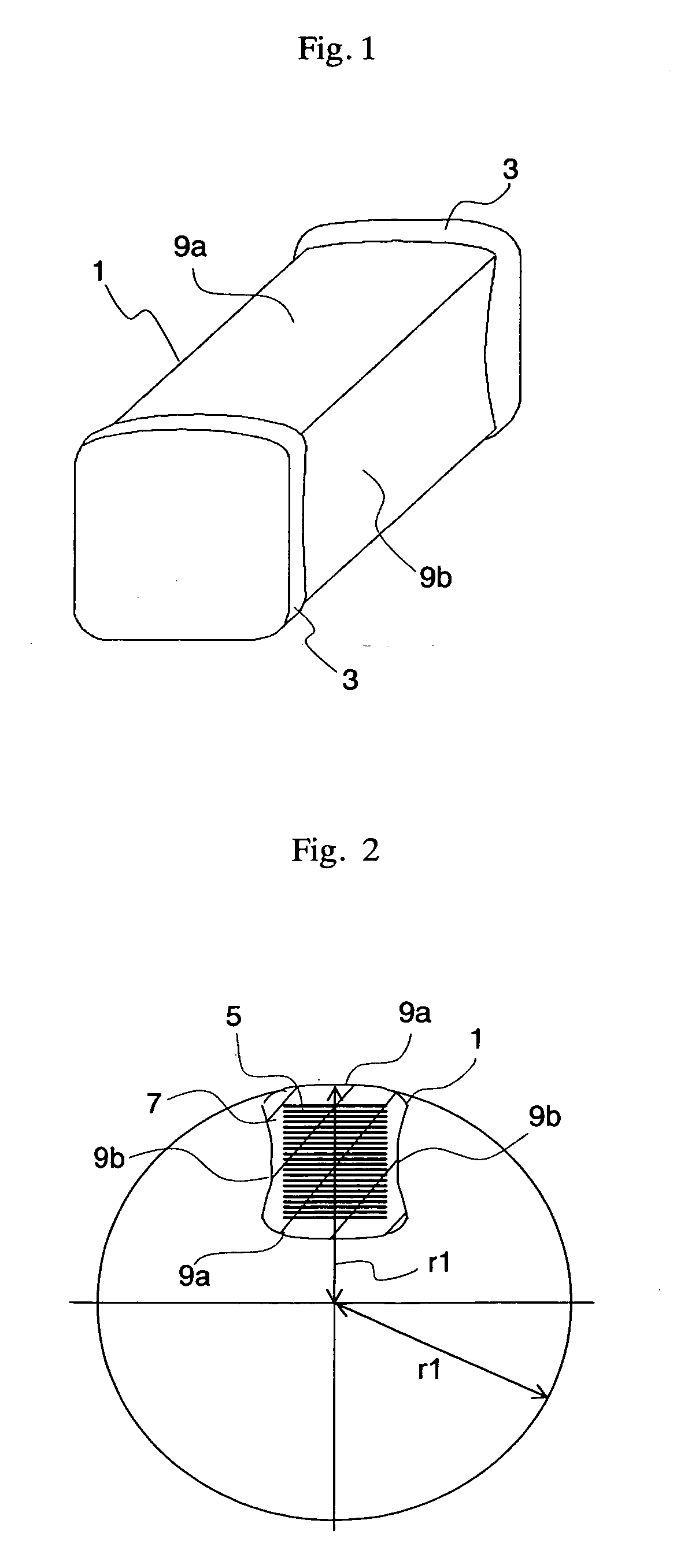
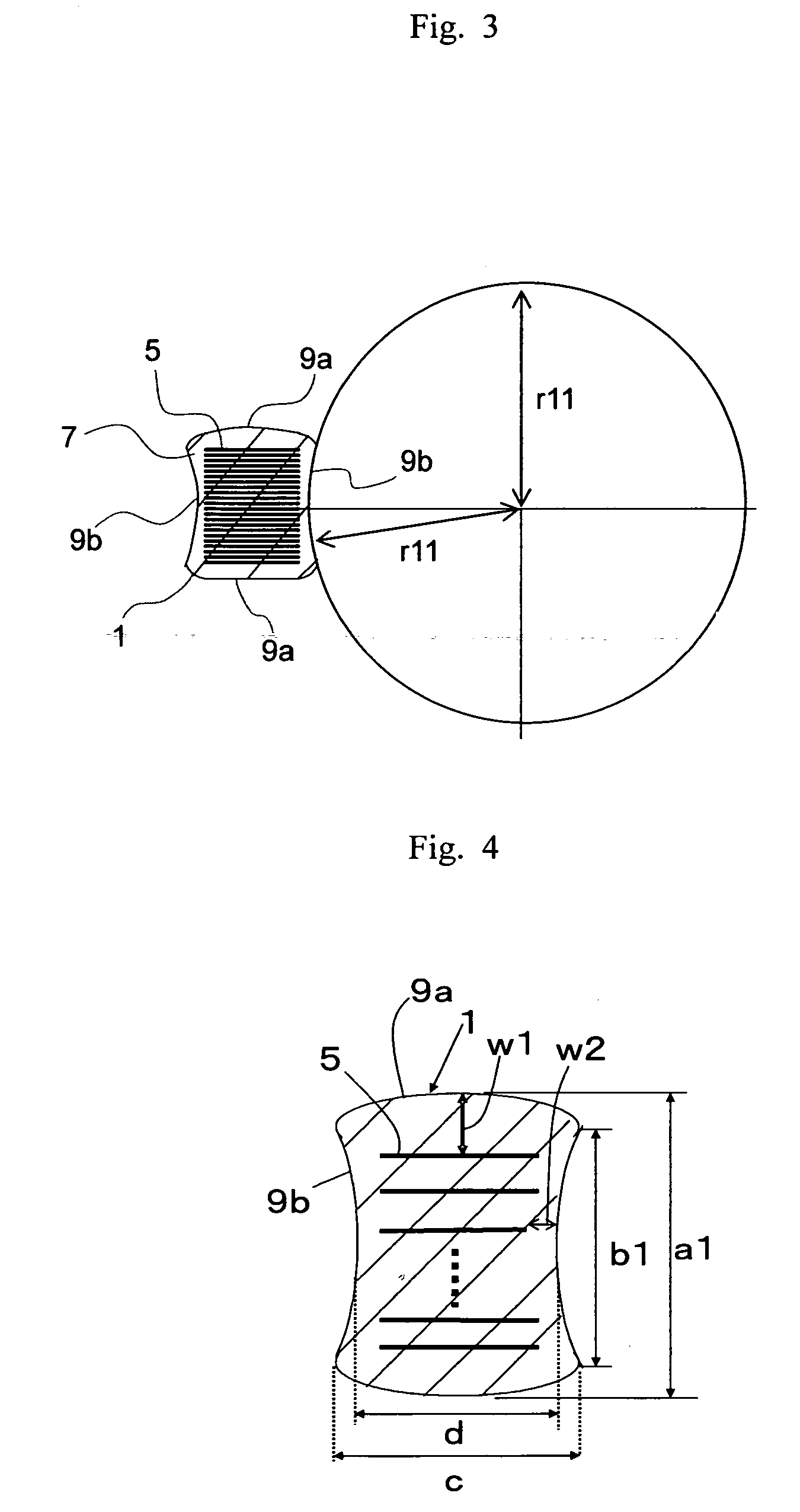
[0037] A chip-type electronic component of the present invention, in particular, taking a multilayer ceramic capacitor as example, will next be described in detail with reference to the accompanying drawings. FIG. 1 is a schematic perspective view of a chip-type electronic component according to this preferred embodiment. FIG. 2 is a schematic sectional view for explaining a radius of curvature r1 of a convexly curved surface. FIG. 3 is a schematic sectional view for explaining a radius of curvature r11 of a concavely curved surface.

[0038] This chip-type electronic component has a pair of external electrodes 3 at end portions of a ceramic body 1 and a conductor part 5 at its interior, and it presents a rectangular solid appearance under bird's eye viewing. In the present invention, a surface (one surface or both surfaces) in a thickness direction (laminate direction) of the ceramic body 1 is convexly curved, and both side surfaces are concavely curved with respect to the convex sur...

second preferred embodiment

[0050] A chip-type electronic component according to other preferred embodiment of the present invention, in particular, taking a multilayer ceramic capacitor as example, will next be described in detail with reference to the accompanying drawings. FIG. 6 is a perspective view showing the chip-type electronic component of this preferred embodiment, and FIG. 7 is its schematic sectional view. This chip-type electronic component has a conductor part 25, which is disposed via an insulating layer 24 in the interior of a ceramic body 21, and a pair of external electrodes 23, 23 at its end portions. This chip-type electronic component presents a rectangular solid appearance under bird's eye viewing. It is especially important that at least one surface containing a long edge side 27 of the ceramic body 21 has a convexly curved surface 29. In this preferred embodiment, the convexly curved surface 29 is formed only on the upper surface of the ceramic body 21. The above-mentioned surface is t...

third preferred embodiment

[0062] A still other preferred embodiment of the present invention, in particular, taking a multilayer ceramic capacitor as example, will next be described in detail with reference to the accompanying drawings. FIG. 11 is a schematic sectional view showing a chip-type electronic component of this preferred embodiment.

[0063] As shown in FIG. 11, this chip-type electronic component has a ceramic body 45, which is formed by laminating alternatively a plurality of insulating layers 41 composed of ceramic (ceramic layers) and conductor layers 43. A pair of external electrodes 49, 49, in which the conductor layers 43 are connected alternately, are formed on both end surfaces 47 of the ceramic body 45, respectively.

[0064] In this preferred embodiment, a thickness t in a laminate direction at a central part 51 between the external electrodes 49 of the ceramic body 45 is greater than a thickness t1 on the end surface 47. Specifically, it is more preferable to satisfy the following relation...


PUM


Abstract

In a chip-type electronic component of the present invention, at least one surface of a ceramic body is a convexly curved surface. Specifically, at least one surface in a thickness direction of the ceramic body may be convexly curved, and the side surface of the ceramic body may be concavely curved. Alternatively, only one surface may be a convexly curved surface. This chip-type electronic component has a high visibility and a high mechanical strength, though it is small. Moreover, in a chip-type electronic component comprising a ceramic body that is formed by alternately laminating insulating layers and conductor layers, and a pair of external electrodes, the thickness in a laminate direction at the central part between external electrodes of the ceramic body is made greater than the thickness of the end surface. This prevents breakage of the external electrodes and also enlarges the ceramic body.

Description

BACKGROUND OF THE INVENTION [0001] 1. Field of the Invention [0002] The present invention relates to chip-type electronic components and, in particular, small chip-type electronic components in the shape of an approximately rectangular solid, such as multilayer ceramic capacitors, inductors, resistors and semiconductor elements. [0003] 2. Description of Related Art [0004] Recently, attempts to miniaturize electronic equipment and achieve high densification of mounting are being pursued. For example, as described in Japanese Patent Application Laid-Open Publication No. 2003-318312, chip-type electronic components having different characteristics, such as a capacitor, an inductor, a resistor, a semiconductor element, are mounted together on a substrate constituting the electronic equipment. As such a chip-type electronic component described in this publication (corresponding to a circuit element of Japanese Patent Application Laid-Open Publication No. 2003-318312), there is a small mu...

Claims


Application Information

Patent Timeline
IPC IPC(8): H01C1/02H01C7/18H01G2/10H01G4/008H01G4/30
CPCH01C1/02H01G4/30H01G2/10H01C7/18H01G4/232
Inventor YAMAZAKI, YOUICHI
Owner KYOCERA CORP
Why Eureka
Try Eureka