Semiconductor device and method of manufacturing the same

Inactive Publication Date: 2005-12-01
KK TOSHIBA
View PDF8 Cites 16 Cited by
  • Summary
  • Abstract
  • Description
  • Claims
  • Application Information

AI Technical Summary

Benefits of technology

[0015] Accordingly, an object of the present invention is to provide a semiconductor device which makes it possible to improve manufacturing yield and reliability in a connecting process between a semiconductor el

Problems solved by technology

However, since the low-k material having holes inside is weak in mechanical strength, a semiconductor element having a low-k film has a disadvantage of easily generating cracking, delaminating, or the like due to the low-k film when the flip chip connection is used.
However, since the low-k film is low in mechanical strength, crack and delamination is easily generated by stress based on the deformation of the solder bumps 5.
With such a connection structure, it is impossible to adequately cope with increasing terminals and becoming finer pitches of semiconductor elements.
However, no consideration is given to deformation of the A

Method used


Image

  • Semiconductor device and method of manufacturing the same
  • Semiconductor device and method of manufacturing the same
  • Semiconductor device and method of manufacturing the same

Examples


Example

[0029] Embodiments of the present invention will be explained with reference to the drawings as follows. It should be noted that though embodiments of the present invention will be described hereinafter based on the drawings, but these drawings are presented only for the illustrative purpose and the present invention is not limited to the drawings.

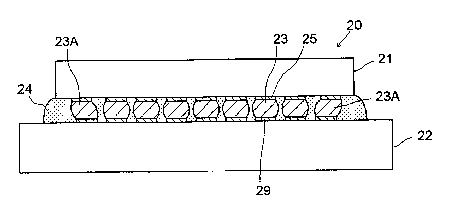
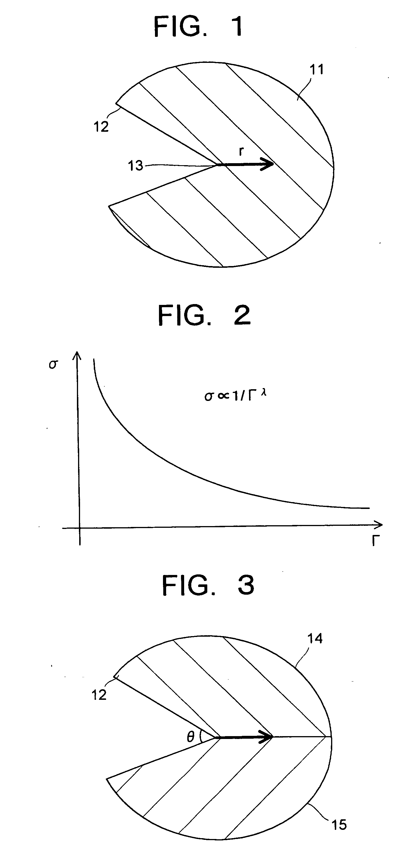
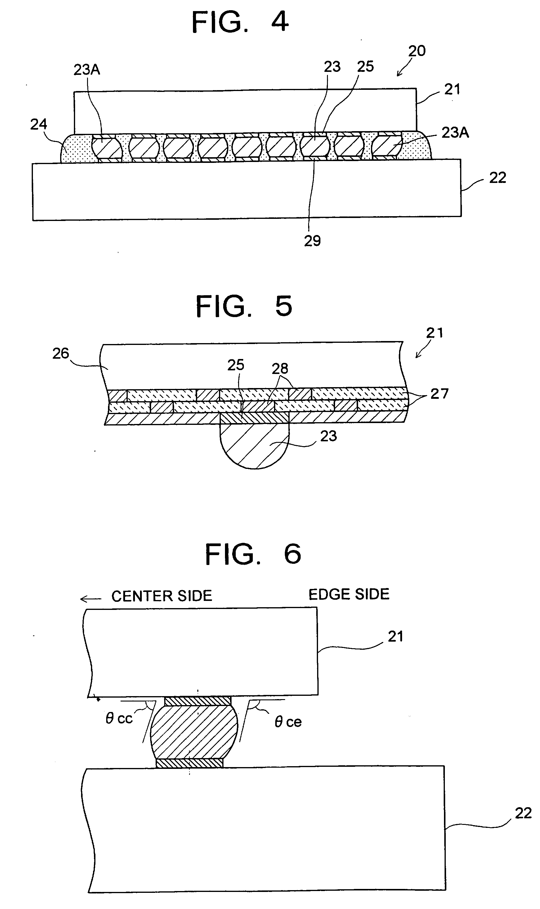
[0030] In a semiconductor device (semiconductor module) relating to an embodiment of the present invention, a semiconductor element (semiconductor chip) mounted on a substrate is provided with a element body having an insulating film with a low dielectric constant, a group of electrode pads having first electrode pads arranged on the element body, and a group of solder bumps having solder bumps formed on the first electrode pads respectively. The group of solder bumps has a solder bump in which the stress intensity factor in the notch shape formed by the first electrode pad and the outline of the solder bump, in a cross section through th...


PUM


Abstract

A semiconductor device comprises a semiconductor element having first electrode pads and solder bumps, and a substrate having second electrode pads connected to the first electrode pads via the solder bumps. The semiconductor element has an insulating film with a low dielectric constant. The group of the solder bumps is provided with a solder bump in which a stress intensity factor K in a notch shape formed by the first electrode pad and the outline of the solder bump, when looking at a cross section through the center of the first electrode pad and the solder bump, is such that on the chip edge side it is less than or equal to its value on the chip center side. Thereby, cracking or delamination of the semiconductor element due to the insulating film with a low dielectric constant can be restrained.

Description

CROSS-REFERENCE TO THE INVENTION [0001] This application is based upon and claims the benefit of priority from the prior Japanese Patent Application No. 2004-160322, filed on May 28, 2004; the entire contents of which are incorporated herein by reference. BACKGROUND OF THE INVENTION [0002] 1. Field of the Invention [0003] The present invention relates to a semiconductor device to which a flip chip connection is applied, and a method of manufacturing the same. [0004] 2. Description of the Related Art [0005] In recent years, in order to cope with increasing terminals, finer pitches, higher signal speed, higher heat generation and so on of semiconductor elements (semiconductor chips), a flip chip connection is used as a mounting system having short wiring and connection lengths. A semiconductor element used to the flip chip connection has electrode pads formed in an area array, for instance, and solder bumps formed on these electrode pads. A substrate on which a semiconductor element i...

Claims


Application Information

Patent Timeline
IPC IPC(8): H01L21/60H01L21/44H05K3/34
CPCH01L23/49816H01L2924/3511H01L24/81H01L2224/13099H01L2224/13111H01L2224/81801H01L2924/01013H01L2924/01029H01L2924/01051H01L2924/01058H01L2924/01079H01L2924/01082H01L2924/01322H01L2924/09701H01L2924/30105H05K3/3436H05K2201/094H05K2201/09427H05K2203/0465H01L2924/01005H01L2924/01006H01L2924/01019H01L2924/01021H01L2924/01033H01L2924/01043H01L2924/0105H01L2924/01075H01L2924/014H01L2224/16105H01L24/17H01L24/05H01L2224/05124H01L2224/05147H01L2224/05556H01L2224/05573H01L2224/05655H01L2224/05664H01L2224/05666H01L2224/0615H01L2224/16225H01L2224/17051H01L2224/171H01L2224/17179H01L2224/32225H01L2224/73204H01L2924/15787Y02P70/50H01L2924/00H01L2924/00012H01L2924/00014
Inventor SAWADA, KANAKOLIJIMA, TOSHITSUNEHOMMA, SOICHI
Owner KK TOSHIBA
Why Eureka
Try Eureka