Chip bonding process

a technology of chip and bonding process, which is applied in the direction of semiconductor/solid-state device details, electrical equipment, semiconductor devices, etc., can solve the problems of low productivity and introduction of a great deal of design limitation

Active Publication Date: 2005-12-01
QUALCOMM INC
View PDF52 Cites 98 Cited by
  • Summary
  • Abstract
  • Description
  • Claims
  • Application Information

AI Technical Summary

Benefits of technology

[0011] Therefore, one objective of the present invention is to provide a chip bonding process. The underfill contaminating the pads of the lower wafer adjacent to the underfill can be avoided. It is not necessary to change the layout of the pads of the lower wafer for avoiding the underfill contaminating the pads of the lower wafer.
[0012] Therefore, another objective of the present invention is to provide a chip bonding process capable of enhancing the productivity.

Problems solved by technology

This will introduce a great deal of limitation to the design for relocating the chip pad 122 of the chip 120.
As a result, low productivity can be expected.

Method used


Image

  • Chip bonding process
  • Chip bonding process
  • Chip bonding process

Examples


first embodiment

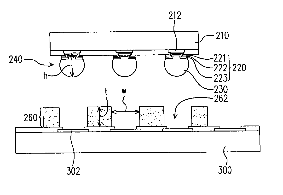
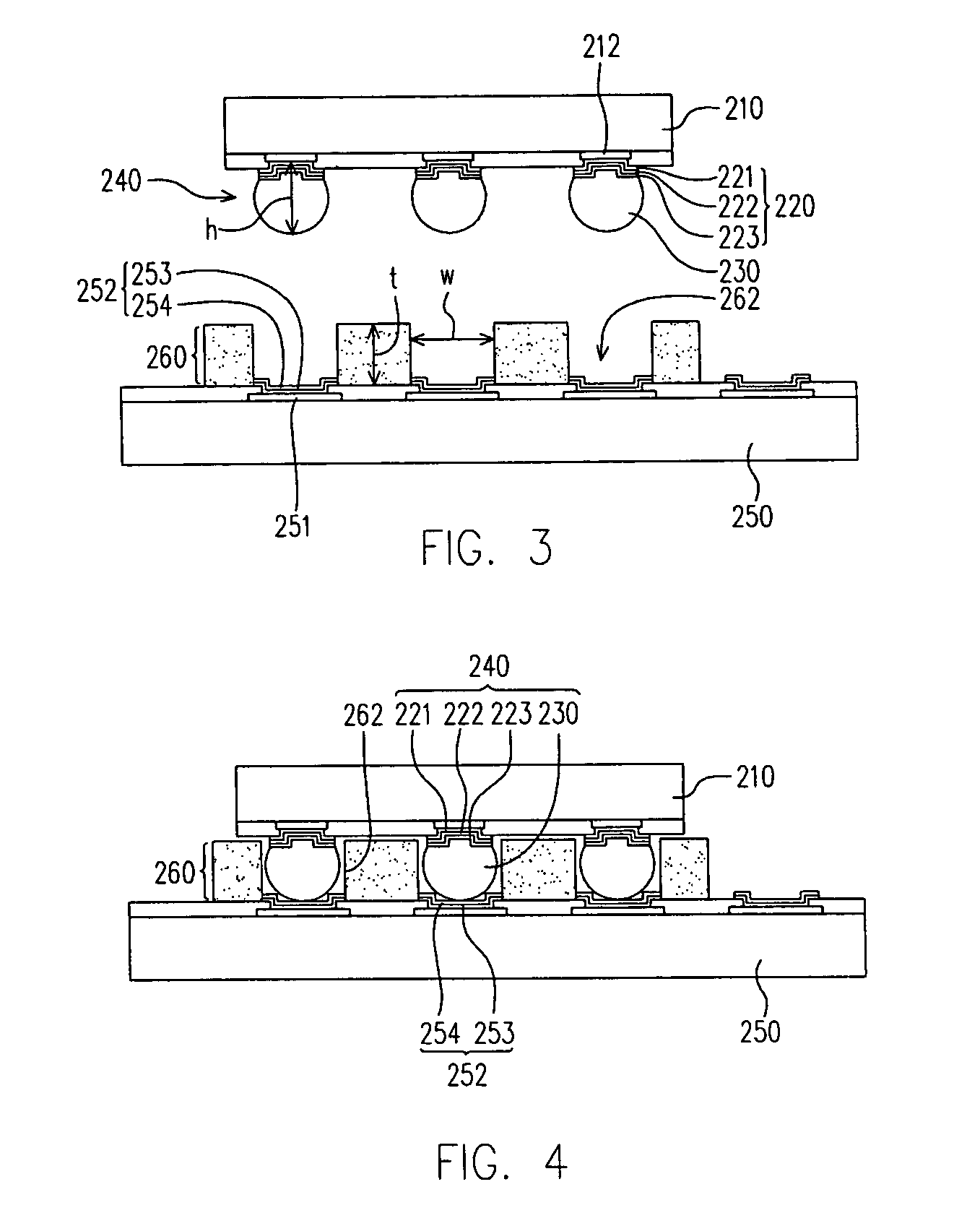
[0022] Referring to FIGS. 3-5, cross-sectional views showing a chip bonding process according to a first preferred embodiment, multiple chips 210 (only one shown in FIGS. 3-5) are provided with a number of aluminium or copper pads 212. The chip 210 comprises a semiconductor substrate with multiple active devices, such as transistor or CMOS, and an interconnecting metallization layer formed on the semiconductor substrate. The pads 212 are connected to the interconnecting metallization layer. Multiple bumps 240 are respectively formed on the pads 212 of the chip 210. The bumps 240 are deposited, for example, by forming a UBM (Under Bump Metallurgy) layer 220 on the pads 212 of the chip 210, followed by forming a solder material 230 on the UBM layer 220 and then performing a reflowing process which makes the solder material 230 ball-shaped, wherein the height h of the bumps 240 ranges from about 5 μm to 400 μm.

[0023] The UBM layer 220 is deposited, for example, by sputtering an adhesi...

second embodiment

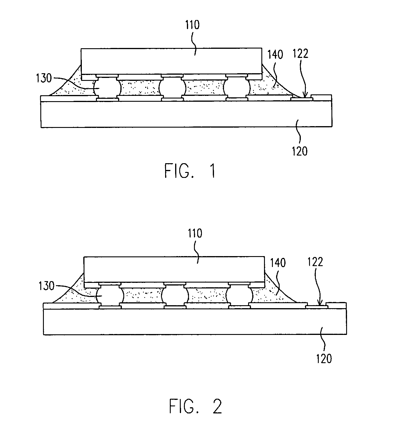
[0037] The process mentioned above is applicable not only to forming an underfill between two chips but also to forming an underfill between a chip and a substrate, as shown in FIG. 6. FIG. 6 is a cross-sectional view showing the bonding of a chip and a substrate according to a second preferred embodiment.

[0038] At first, a number of bumps 240 are formed on the pads 212 of the chip 210. The bumps 240 herein may have the same structure or materials as the bumps 240 described in the first embodiment. Next, a patterned polymer layer 260 is formed on a substrate 300 such as printed circuit board. There are multiple openings 262 formed in the patterned polymer layer 260 and exposing multiple pads 302 of the substrate 300. The patterned polymer layer 260 may have a thickness between about 5 μm and 400 μm and, preferably, between about 10 μm and 100 μm. The structure of the patterned polymer layer 260 and the process for forming the same can be referred to the first embodiment.

[0039] The...

third embodiment

[0040] In the process for forming the underfill mentioned above, each of the openings in the patterned polymer layer exposes only one pad. However, the invention can not be limited to the above embodiments. As shown in FIG. 7, a top view showing an underfill formed on a wafer or a substrate according to a third preferred embodiment, multiple socket-shaped openings 462 are formed in the patterned polymer layer 460. Each of the socket-shaped openings 462 may expose multiple aligned pads 252 of the wafer 250. Alternatively, the openings in the patterned polymer layer may have various shapes. The structure of the patterned polymer layer 460 and the process for forming the same can be referred to the detail of the patterned polymer layer 260 described in the first embodiment. The only difference between the patterned polymer layers 260 and 460 is the shape of the openings 262 and 462.

[0041] The patterned polymer layer 460 described in the third preferred embodiment not only can serve as...


PUM


Abstract

A bonding process includes the following process. A bump is formed on a first electric device. A patterned insulation layer is formed on a second electric device, wherein the patterned insulation layer has a thickness between 5 μm and 400 μm, and an opening is in the patterned insulation layer and exposes the second electric device. The bump is joined to the second electric device exposed by the opening in the patterned insulation layer.

Description

CROSS-REFERENCE TO RELATED APPLICATION [0001] This application claims the priority benefit of Taiwan application serial no. 93112610, filed on May 5, 2004. All disclosure of the Taiwan application is incorporated herein by reference. BACKGROUND OF THE INVENTION [0002] 1. Field of the Invention [0003] The invention relates to a chip bonding process, and more particularly to a process for a patterned underfill being formed in advance of bonding chips. [0004] 2. Description of the Related Art [0005] IT products are playing a more and more important role in modern industrial society recently. The function of electronic products becomes much more versatile as the trend renews old-fashion IT products. Their qualities are becoming more stable as well. When it comes to package technology, in order to possess better performance in electric conduction and thermal conduction, Flip Chip Package is the common option and it occupies less package volume. [0006] Referring to FIG. 1 and FIG. 2, cros...

Claims


Application Information

Patent Timeline
Patent Type & Authority Applications(United States)
IPC IPC(8): H01L21/44H01L21/48H01L21/50H01L21/56H01L21/60H01L21/98H01L23/485H01L25/065
CPCH01L21/563H01L24/16H01L24/81H01L24/94H01L25/0657H01L25/50H01L2224/1308H01L2224/13083H01L2224/13111H01L2224/13147H01L2224/13155H01L2224/16145H01L2224/16225H01L2224/16237H01L2224/73203H01L2224/73204H01L2224/81191H01L2224/8121H01L2224/81815H01L2224/83192H01L2224/83194H01L2224/83907H01L2225/06513H01L2225/06527H01L2924/01013H01L2924/01022H01L2924/01029H01L2924/01047H01L2924/0105H01L2924/01073H01L2924/01074H01L2924/01079H01L2924/01082H01L2924/04953H01L24/13H01L2924/00013H01L2924/01006H01L2924/01024H01L2924/01033H01L2924/014H01L2924/0133H01L24/29H01L2224/32225H01L2924/0132H01L24/83H01L2224/29111H01L2224/2919H01L2224/29012H01L2224/29011H01L2924/00014H01L2224/13099H01L2924/00H01L2224/29099H01L2924/00012H01L24/05H01L24/11H01L2224/05001H01L2224/05022H01L2224/05027H01L2224/05147H01L2224/05166H01L2224/05171H01L2224/05572H01L2224/05655H01L2224/0615H01L2224/13022H01L2224/8114
Inventor LIN, MOU-SHIUNGLIN, SHIH HSIUNGLO, HSIN-JUNG
Owner QUALCOMM INC
Why Eureka
Try Eureka