Display panel and method for manufacturing display panel

a display panel and manufacturing method technology, applied in the direction of discharge tube luminescnet screens, discharge tube/lamp details, electric discharge lamps, etc., can solve the problems of varying the distance between the substrates, difficulty in precisely determining the line width and position, etc., to achieve low moisture permeability, reliably prevent moisture intrusion into the inside, and small area

Active Publication Date: 2005-12-08
SANYO ELECTRIC CO LTD
View PDF2 Cites 34 Cited by
  • Summary
  • Abstract
  • Description
  • Claims
  • Application Information

AI Technical Summary

Benefits of technology

[0009] According to the present invention, a pixel substrate and a sealing substrate are joined using a metal solder. A metal has a very low permeability of moisture, and therefore, can reliably prevent intrusion of moisture into the inside and allows reduction of an amount of desiccant to be provided in the inside space, or, omission of such a desiccant. In addition, because a joint solder layer is formed through patterning, it is possible to very precisely form the solder layer. Therefore, the large margin for the joining area is no longer necessary, which allows for reliable sealing with a small area, an increase in a display region which actually realizes a display, and a reduction in the size of the display. Moreover, because the solder layer can be precisely formed, it is possible to prevent variation in the distance between substrates.

Problems solved by technology

However, in such joining, it is difficult to precisely determine a line width and a position of the low-melting-point glass, and therefore, a sufficient margin must be provided in the joining portion.
There is another problem in that a distance between the substrates varies when an amount of the low-melting-point glass changes.

Method used


Image

  • Display panel and method for manufacturing display panel
  • Display panel and method for manufacturing display panel
  • Display panel and method for manufacturing display panel

Examples


Embodiment Construction

[0014] Preferred embodiments (hereinafter, referred to simply as “embodiment”) of the present invention will now be described referring to the drawings.

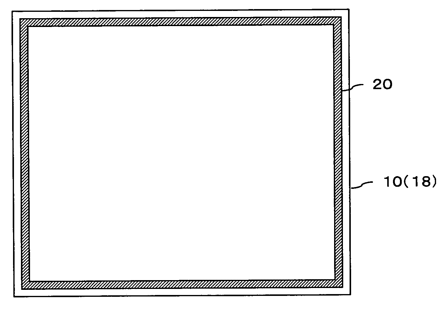
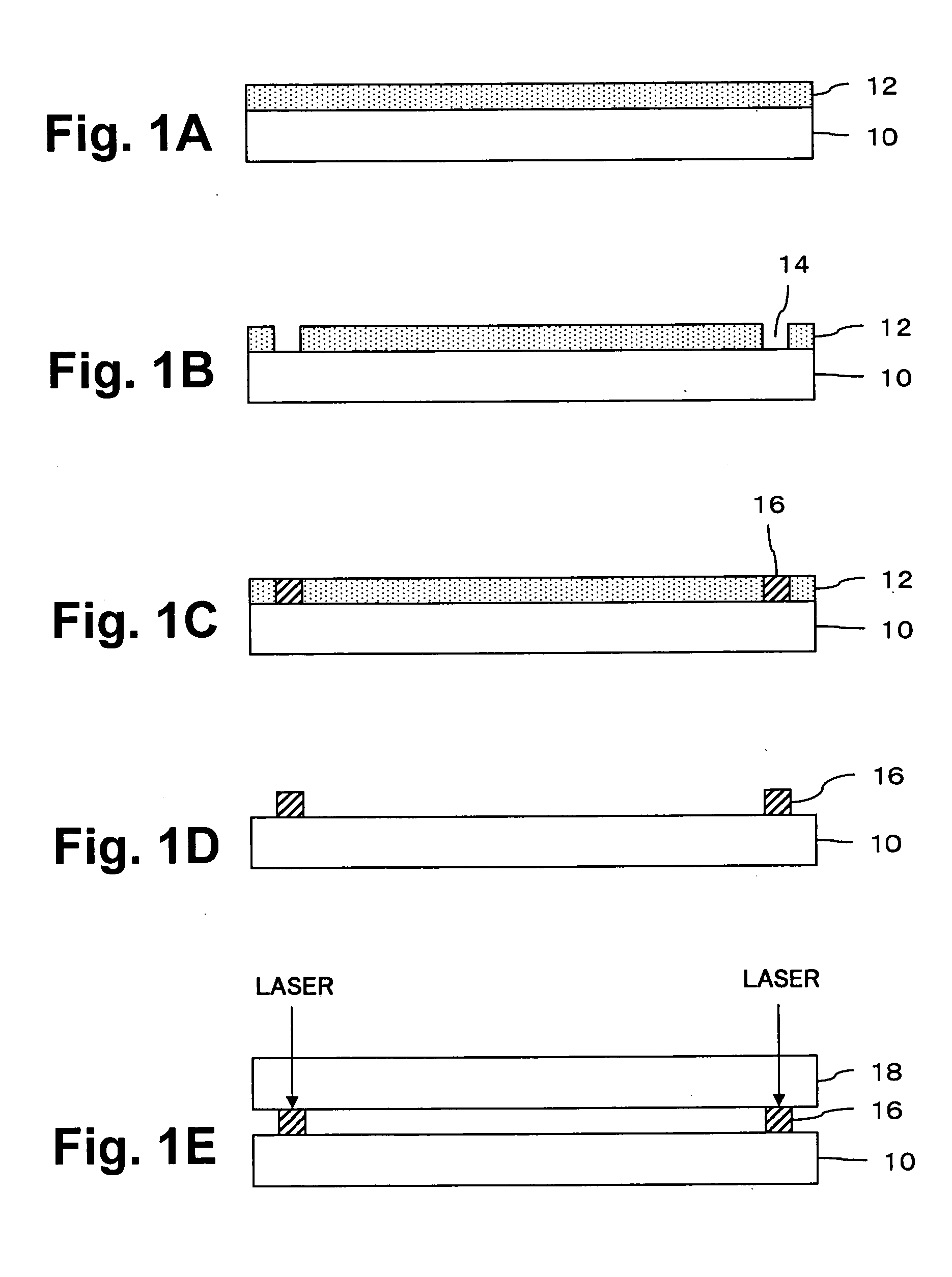
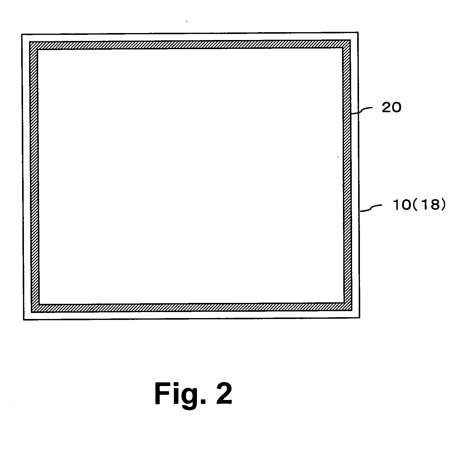
[0015] FIGS. 1(a) through 1(e) show a procedure for joining substrates according to a preferred embodiment of the present invention. A mask film 12 is formed on a front surface of a sealing substrate 10 which is made of glass (FIG. 1(a)). As the mask film 12, a photosensitive resin which can withstand a temperature of approximately 200° C. is used. For example, a resin which is used for a color filter in the organic EL panel, an organic material which is used for an acrylic planarization film in the organic EL panel, or an inorganic material such as SiO2 and SiN is used.

[0016] The mask film 12 is then exposed through a mask pattern and is developed, so that a frame-shaped groove 14 corresponding to the mask pattern is formed (FIG. 1(b)). Because the groove 14 is formed through photolithography, the precision of the groove 14 is ver...


PUM

PropertyMeasurementUnit
temperatureaaaaaaaaaa
melting pointaaaaaaaaaa

Abstract

A metal solder layer is formed on a sealing substrate through patterning. A pixel substrate is overlapped to the sealing substrate and the solder layer is irradiated with laser so that the sealing substrate and the pixel substrate are connected. Because the joining is achieved by the metal solder layer, intrusion of moisture into the inside space can be reduced. In addition, the solder layer can be very precisely formed through patterning.

Description

CROSS-REFERENCE TO RELATED APPLICATIONS [0001] The entire disclosure of Japanese Patent Application No. 2004-55971 including specification, claims, drawings and abstract is incorporated herein by reference. BACKGROUND OF THE INVENTION [0002] 1. Field of the Invention [0003] The present invention relates to manufacture of a display panel such as an organic electroluminescence (hereinafter simply referred to as “EL”) display panel and, in particular, to a sealing structure in the display panel. [0004] 2. Description of the Related Art [0005] Plasma display panels (PDP) and liquid crystal display devices (LCD) are becoming widely available as thin flat display panels and organic EL panels are commercially available. [0006] In an organic EL panel, an organic material is used as a light emitting material in each pixel or the like. Because the lifetime of the organic material is shortened when the organic material contains moisture, it is necessary to minimize an amount of moisture in a s...

Claims


Application Information

Patent Timeline
Patent Type & Authority Applications(United States)
IPC IPC(8): H01J1/62H01J63/04H05B33/04H01L51/50H01L51/52H05B33/10H05B33/14
CPCH01L51/5237H10K50/8423H10K50/8426H01L2924/12044H10K71/233
Inventor NISHIKAWA, RYUJIOMURA, TETSUJINAKAI, MAASAYA
Owner SANYO ELECTRIC CO LTD
Why Eureka
Try Eureka