Lithographic apparatus and device manufacturing method

a technology of lithographic projection and manufacturing method, which is applied in the direction of photomechanical equipment, instruments, optics, etc., can solve the problems of specific lithographic errors in the patterned layer, the general complexity of the illumination system and the difficulty of achieving the effect of reducing the cost of the lithographic projection system

Inactive Publication Date: 2005-12-08
ASML NETHERLANDS BV
View PDF28 Cites 64 Cited by
  • Summary
  • Abstract
  • Description
  • Claims
  • Application Information

AI Technical Summary

Benefits of technology

[0024] Although specific reference may be made in this text to the use of the apparatus according to the invention in the manufacture of ICs, it should be explicitly understood that such an apparatus has many other possible applications. For example, it may be employed in the manufacture of integrated optical systems, guidance and detection patterns for ma

Problems solved by technology

To meet the above-mentioned requirements, the illumination system of a lithographic projection system is generally quite complex.
The illumination systems discussed above still suffer from various problems, however.
Both types of errors are referred to as “ellipticity of the radiation beam” or simply as “ellipticity error,” and typically lead to specific lithographic errors in the patterned layers.
For other settings, the integrator entrance face may also be over-filled, leading to energy wastage.
Additionally, 157 nm excimer lasers and other excimer lasers tend to have large divergence differences in X and Y directions which cannot be completely resolved using beam expander lenses while keeping the shape of the beam within acceptable dimensions.
Ellipticity errors in the radiation beam may also be caused by subsequent elements, such as the mask and elements of the projection system.
Current lithographic apparatus do not correct or compensate for ellipticity errors introduced into the ra

Method used


Image

  • Lithographic apparatus and device manufacturing method
  • Lithographic apparatus and device manufacturing method
  • Lithographic apparatus and device manufacturing method

Examples


Embodiment Construction

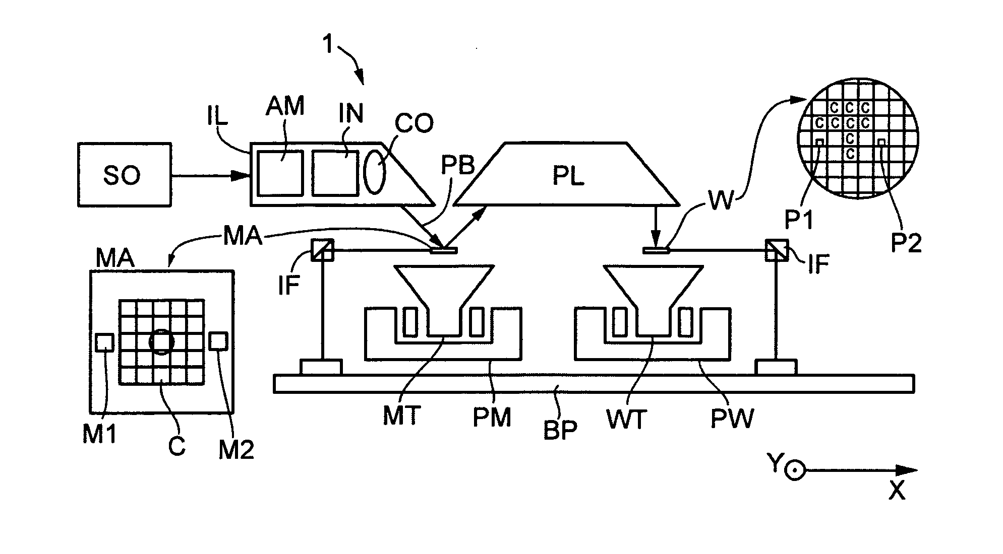
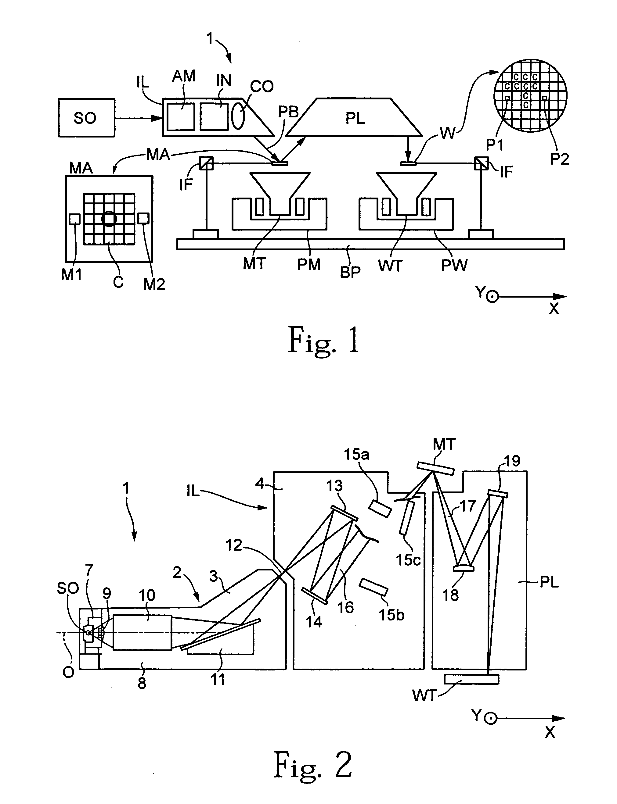
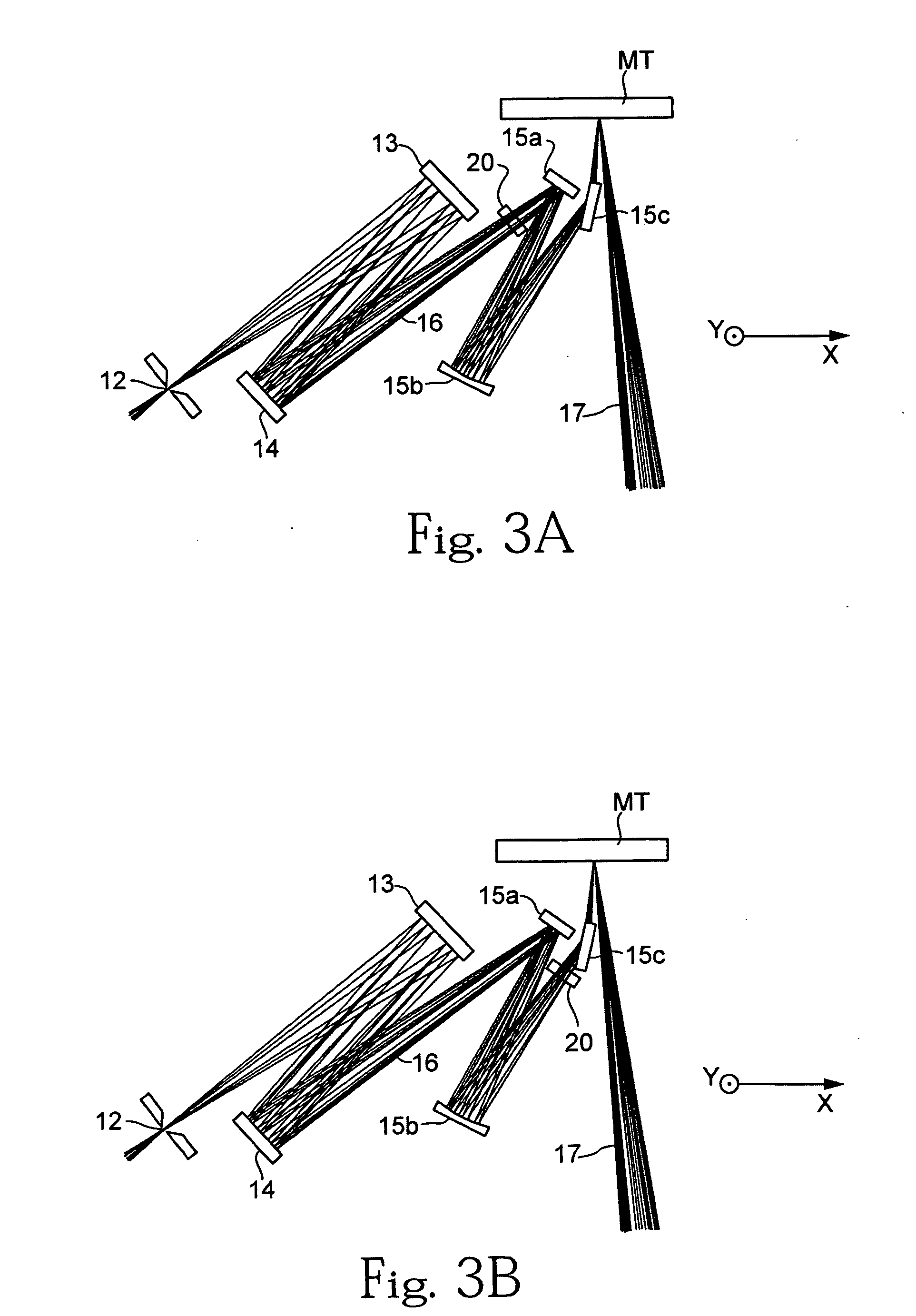
[0053]FIG. 1 schematically depicts a lithographic projection apparatus 1 according to an embodiment of the invention. The apparatus 1 includes a base plate BP. A illumination system is configured to supply a beam PB of radiation (e.g. EUV radiation). A radiation source SO is configured to provide radiation to the illumination system IL. The source SO and the apparatus 1 may be separate, for example when the source is a plasma discharge source. In such case, the source SO is not considered to form part of the apparatus 1 and the radiation beam is generally passed from the source LA to the illumination system IL with the aid of a radiation collector including, for example, suitable collecting mirrors and / or a spectral purity filter. In other cases, the source SO may be integral with the apparatus 1, for example when the source SO is a mercury lamp. The present invention encompasses both of these scenarios. The source SO and the illumination system IL may be referred to as a radiation ...


PUM


Abstract

A lithographic apparatus includes an illumination system including a field faceted mirror including a plurality of field facets and configured to receive radiation from a radiation source and form a plurality of images of the radiation source on corresponding pupil facets of a pupil faceted mirror. Each of the field facets is configured to provide an illumination slit at a level of a patterning device. The illumination slits are summed together at the level of the patterning device to illuminate the patterning device. First blades are configured to block radiation from a radiation source and each first blade is selectively actuable to cover a portion of a selectable number of field facets. The field faceted mirror further comprises partial field facets, the partial field facets being configured to produce a partial illumination slit at the level of the patterning device, and the pupil faceted mirror further includes pupil facets corresponding to the partial field facets. The partial field facets are configured to produce an illumination slit that is summed with the summed illumination slits of the field facets and/or correct for non-uniformity in the summed illumination slits of the field facets. Second blades are selectively actuable to cover a portion of a selectable number of partial field facets.

Description

CROSS REFERENCE TO RELATED APPLICATIONS [0001] This application is a continuation-in-part of co-pending U.S. application Ser. No. 10 / 784,895, filed Feb. 24, 2004 and entitled “LITHOGRAPHIC APPARATUS AND DEVICE MANUFACTURING METHOD,” which is a continuation-in-part of U.S. application Ser. No. 10 / 388,766, filed Mar. 17, 2003 and entitled “LITHOGRAPHIC APPARATUS AND DEVICE MANUFACTURING METHOD,” now U.S. Pat. No. 6,771,352, issued Aug. 3, 2004, which claims priority from European Application No. 02251933.4, filed Mar. 18, 2002, the entire contents of each of which are herein incorporated by reference. This application incorporates by reference U.S. application Ser. Nos. 10 / 379,999, filed Mar. 6, 2003 and entitled “MASK FOR USE IN LITHOGRAPHY, METHOD OF MAKING A MASK, LITHOGRAPHIC APPARATUS, AND DEVICE MANUFACTURING METHOD,” and 10 / 157,033, filed May 30, 2002 and entitled “LITHOGRAPHIC APPARATUS, DEVICE MANUFACTURING METHOD, DEVICE MANUFACTURED THEREBY, CONTROL SYSTEM, COMPUTER PROGRAM...

Claims


Application Information

Patent Timeline
IPC IPC(8): G03B27/54G03F7/20
CPCG03F7/70075G03F7/70091G03F7/702G03F7/70191G03F7/70108
Inventor DIERICHS, MARCEL MATHIJSBOTMA, HAKOEURLINGS, MARKUS FRANCISCUS ANTONIUS
Owner ASML NETHERLANDS BV
Why Eureka
Try Eureka