LDMOS device and manufacturing method thereof

A device and local field technology, which is applied in the field of semiconductor integrated circuit manufacturing, can solve the problems of low breakdown voltage, easy breakdown, and current accumulation, so as to reduce the specific on-resistance, adjust the breakdown voltage, and increase the current performance effect

Inactive Publication Date: 2015-02-25
SHANGHAI HUAHONG GRACE SEMICON MFG CORP
View PDF6 Cites 10 Cited by
  • Summary
  • Abstract
  • Description
  • Claims
  • Application Information

AI Technical Summary

Problems solved by technology

The existing first structure will bring the following two problems: the first problem is, if figure 2 As shown, the current path schematic diagram of the existing first LDMOS device, the current path of the LDMOS device will go along the sidewall and bottom of the shallow trench field oxygen 103a in the drain region, so the path of the current will be very long, resulting in drain region The resistance of the LDMOS device is large, and the current in the linear region of the LDMOS device is small, which affects the ability of the LDMOS device
The second question is, if figure 2 As shown, at the corner of the bottom of the shallow trench field oxygen 103a in the drain region, that is, the area A shown in the dotted line box, due to the characteristics of the morphology of the shallow trench field oxygen 103a in the drain region, an angle of 80° to 88° will be formed at the corner of the area A. The existence of this angle will cause the current to accumulate when the current flows through it, which will cause the concentration of the electric field during the withstand voltage, resulting in a lower breakdown voltage; image 3 Shown is the impact ionization simulation diagram of the first existing LDMOS device, and the area A1 shown in the dotted line box is figure 2 The simulation at area A in , the area A2 shown in the dotted line box is an enlarged view of area A1, you can see figure 2 The simulation situation of impact ionization on the corner of area A. The darker the color, the stronger the impact ionization is, that is, the more concentrated the electric field is. Area A is the area where impact ionization is more severe, and the corner of area A is the most powerful. Here The electric field is the most concentrated and the breakdown is most likely to occur
[0003] like Figure 4 Shown is a schematic structural diagram of the existing second LDMOS device; the existing second LDMOS device is a pair of figure 1 The only difference between the optimization of the existing first type of LDMOS device shown and the existing first type of LDMOS device is that the depth of the shallow trench field oxygen 103a in the drain region of the existing second type of LDMOS device is shallower than that used to isolate The depth of the shallow trench field oxygen 103 in the active region, by figure 2 It can be seen that the reduction of the depth of the shallow trench field oxygen 103a in the drain region will make the entire current path of the existing second type LDMOS device shorter than that of the existing first type LDMOS device, which can solve the problem of the existing first type LDMOS device. The first problem exists, but it is also the STI process, the current / electric field concentration problem caused by the region A where the first type of LDMOS device exists, that is, the second problem still cannot be solved

Method used


Image

  • LDMOS device and manufacturing method thereof
  • LDMOS device and manufacturing method thereof
  • LDMOS device and manufacturing method thereof

Examples


Embodiment Construction

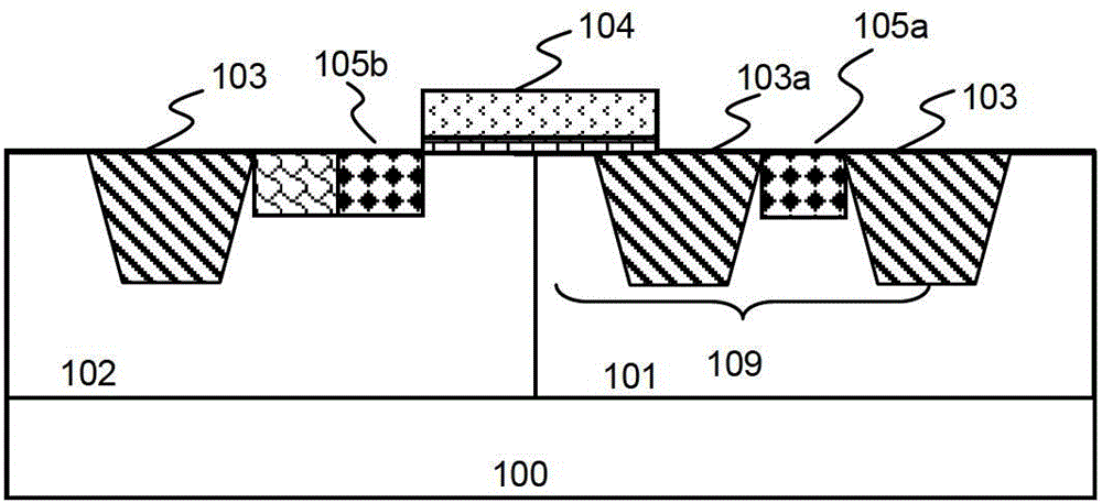
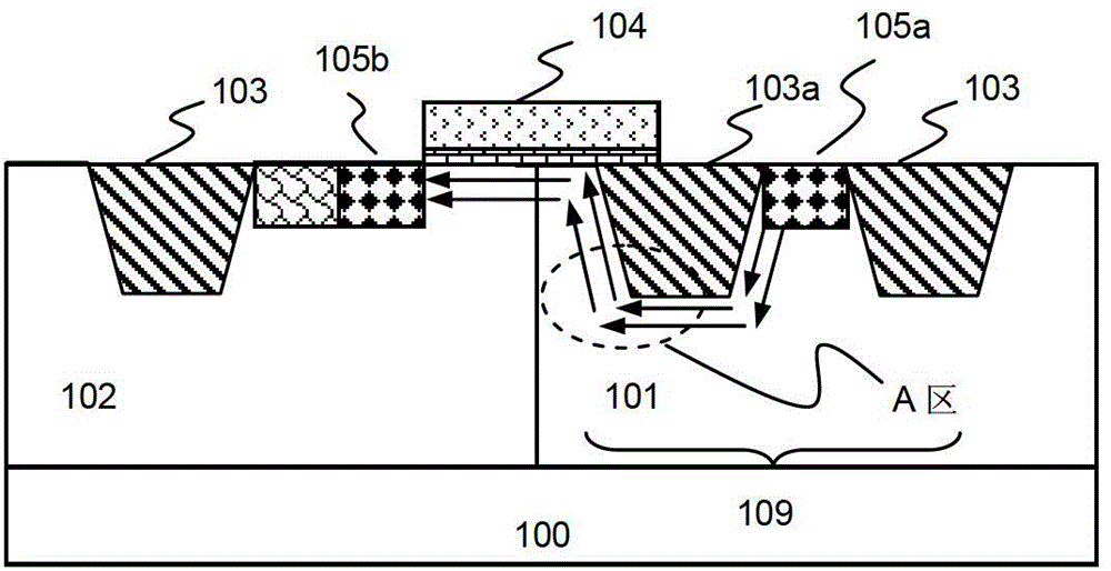
[0044] Such as Figure 5A As shown, it is a schematic structural diagram of an LDMOS device according to an embodiment of the present invention; the LDMOS device according to an embodiment of the present invention is formed on a silicon substrate 200, and the active region is isolated by a shallow trench field oxygen 203, and the LDMOS device includes:

[0045] The drift region 201 is composed of a doped region of the first conductivity type formed in the silicon substrate 200 .

[0046] The channel region 202 is composed of a doped region of the second conductivity type formed in the silicon substrate 200 ; the drift region 201 and the channel region 202 are in lateral contact.

[0047] The polysilicon gate 204 formed above the silicon substrate 200, the polysilicon gate 204 is isolated from the surface of the silicon substrate 200 by a gate dielectric layer such as a gate oxide layer, and the polysilicon gate 204 is isolated from the channel in the lateral direction The reg...


PUM


Abstract

The invention discloses an LDMOS device formed on a silicon substrate. An active area is isolated by a shallow groove field oxide, a partial field oxide is adopted in a drain region field oxide in a drift region between a channel region and a drain region, the partial field oxide is formed by partial field oxidation after silicon in the partial field oxide region is etched by a certain depth, and the depth of the partial field oxide is defined by the depth of the etched silicon in the partial field oxide region. The invention further discloses a manufacturing method of the LDMOS device. According to the LDMOS device and the manufacturing method of the LDMOS device, a smooth bottom is formed in the drain area through partial field oxide, and therefore the problem that current and an electricity field are centralized at the bottom of the field oxide of the drain region can be solved, and the breakdown voltage of the device can be improved; the length of the current path of the drain region of the device can be shortened, so the specific on-resistance of the device can be lowered, and the current performance of the device can be improved.

Description

technical field [0001] The invention relates to the field of manufacturing semiconductor integrated circuits, in particular to an LDMOS device; the invention also relates to a method for manufacturing the LDMOS device. Background technique [0002] The introduction of Shallow Trench Isolation (STI) technology can effectively shorten the distance between active regions to perform effective field oxygen isolation, which greatly increases the integration level. However, if LDMOS devices are integrated in the STI process, STI also exists in the drain region of the LDMOS device. At this time, due to the shape of the bottom of the STI, the LDMOS device is likely to break down at the bottom of the STI, which reduces the breakdown voltage of the LDMOS device. At the same time, due to the shape of the STI, the current flows along the interface between the STI and the silicon when the LDMOS device is turned on, and the current path Longer, resulting in a higher on-resistance of the LD...

Claims


Application Information

Patent Timeline
Patent Type & Authority Applications(China)
IPC IPC(8): H01L29/78H01L29/08H01L21/336
CPCH01L29/0653H01L29/42368H01L29/66659H01L29/7835H01L29/7816H01L29/0611H01L29/0882H01L29/66681
Inventor 金锋石晶
Owner SHANGHAI HUAHONG GRACE SEMICON MFG CORP
Why Eureka
Try Eureka