

Nanocrystal electroluminescence device and fabrication method thereof
a technology of electroluminescence device and nanocrystal, which is applied in the direction of luminescent composition, thermoelectric device, chemistry apparatus and processes, etc., can solve the problems of low color purity, difficult control of nanocrystal layer thickness and hole transport layer, etc., and achieve the effect of increasing the color purity of the electroluminescence devi
- Summary
- Abstract
- Description
- Claims
- Application Information
AI Technical Summary
Benefits of technology
Problems solved by technology
Method used
Image

Examples
example 1
Fabrication of Electroluminescence Device Employing CdSeS Nanocrystal Light-emitting Layer Dispersed in Octane
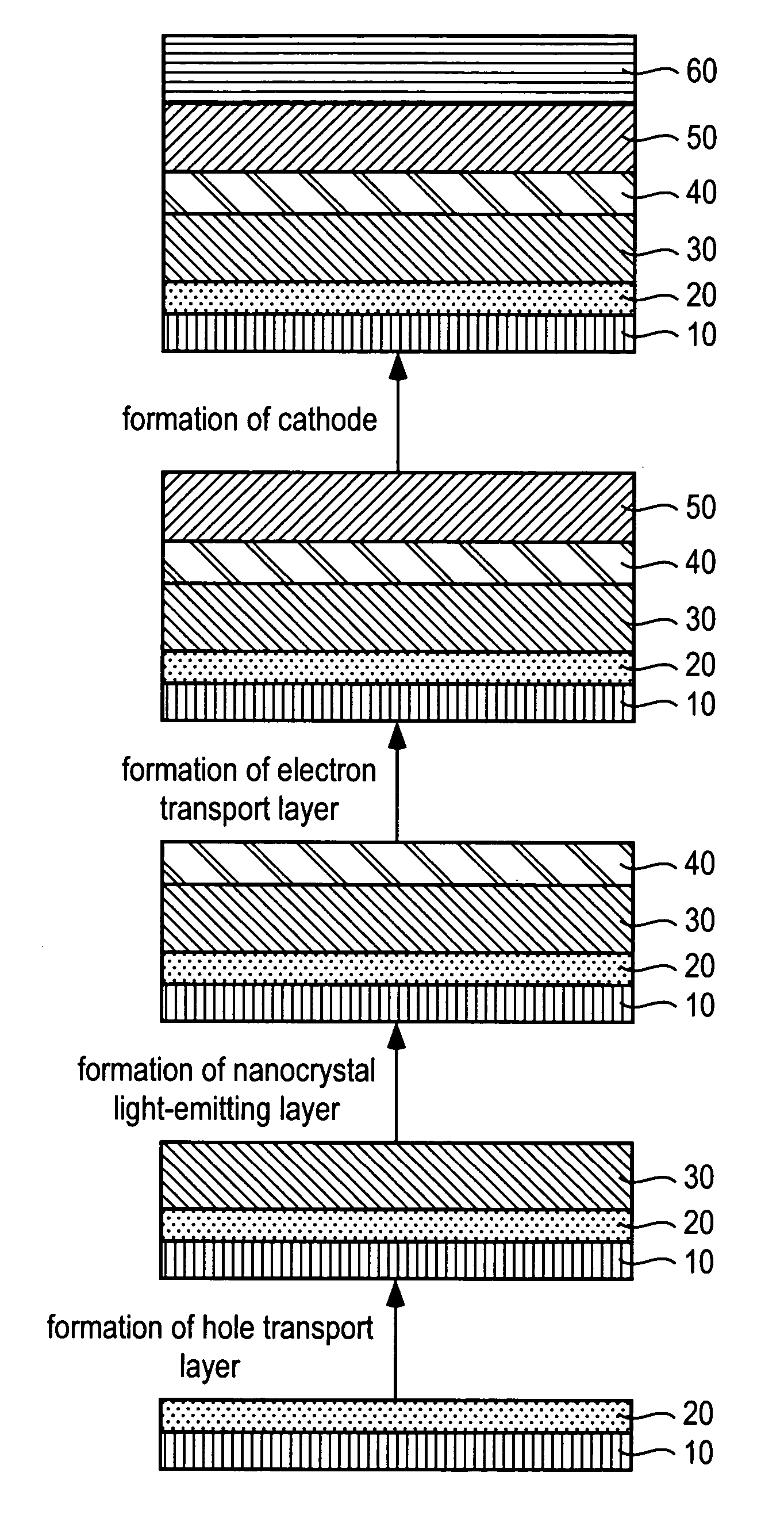
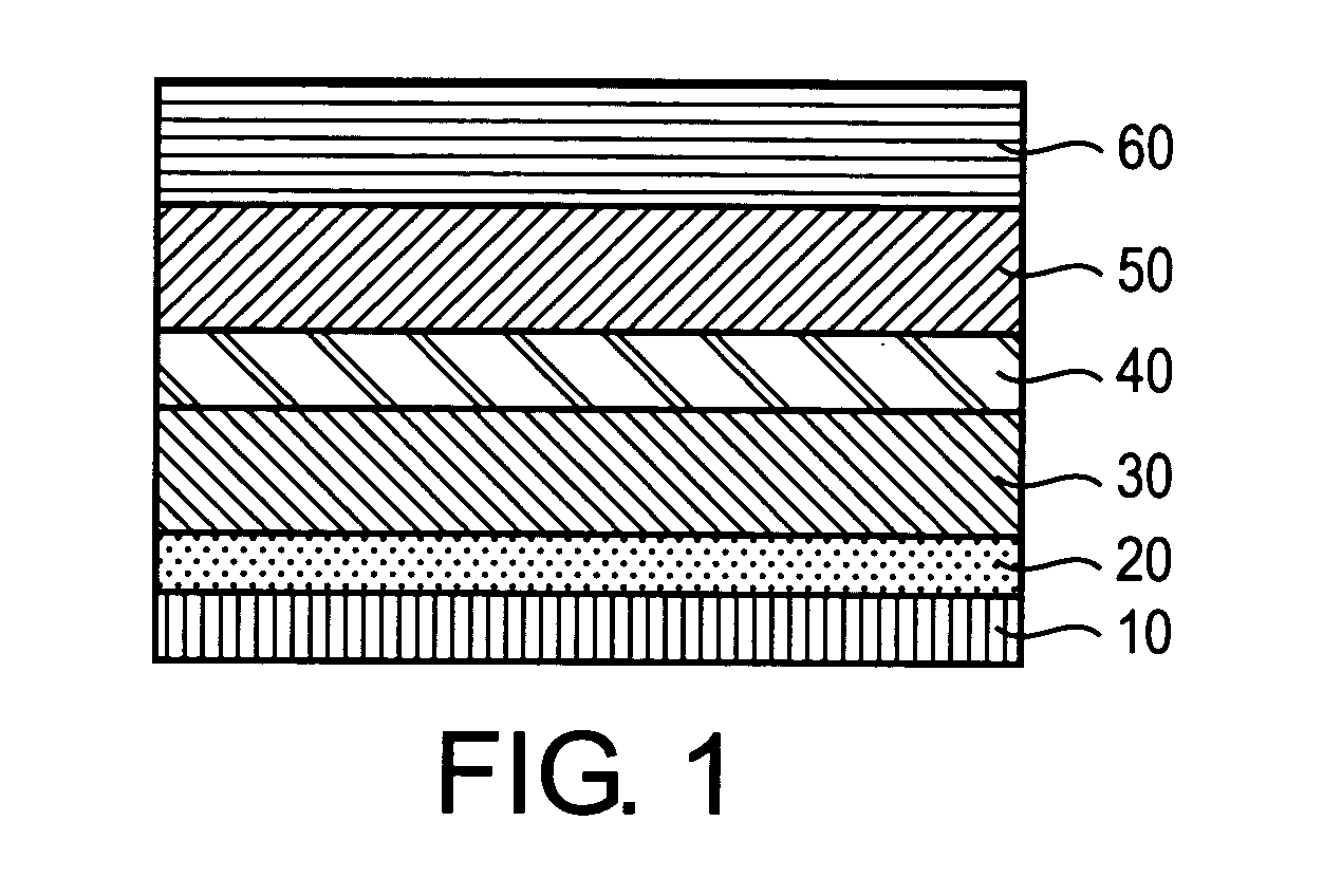
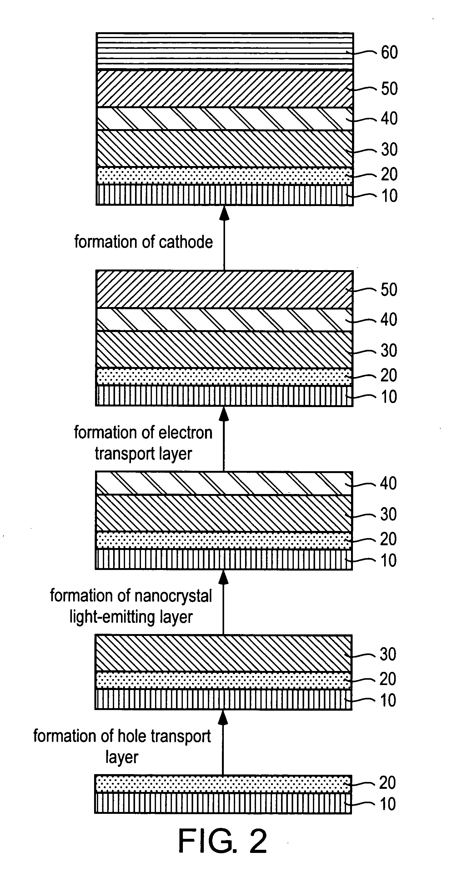
[0055] This example shows the fabrication of an electroluminescence device wherein a nanocrystal light-emitting layer is independently and separately formed. First, an ITO-patterned glass substrate was sequentially washed with a neutral detergent, deionized water, water and isopropyl alcohol, and was then subjected to UV-ozone treatment. A solution of 1 wt % of poly(9,9′-dioctylfluorene-co-N-(4-butylphenyl)diphenylamine (TFB) in chlorobenzene was spin-coated on the ITO-patterned substrate to a thickness of about 50 nm, and then baked at 180° C. for 10 minutes to form a hole transport layer. A dispersion of the CdSeS nanocrystals (1 wt %) prepared in Preparative Example 1 in octane was spin-coated on the hole transport layer, and dried to form a nanocrystal light-emitting layer having a thickness of about 5 nm. At this time, the octane used herein is a solvent which does not...
example 2
Fabrication of Electroluminescence Device Employing CdSeS Nanocrystal Light-emitting Layer Dispersed in Chlorobenzene
[0058] First, an ITO-pattemed glass substrate was sequentially washed with a neutral detergent, deionized water, water and isopropyl alcohol, and was then subjected to UV-ozone treatment. A solution of 1 wt % of poly(9,9′-dioctylfluorene-co-N-(4-butylphenyl)diphenylamine (TFB) in chlorobenzene was spin-coated on the ITO-patterned substrate to a thickness of about 50 nm, and then baked at 180° C. for 10 minutes to form a hole transport layer. A dispersion of 1 wt % of the CdSeS nanocrystals prepared in Preparative Example 1 in chlorobenzene was spin-coated on the hole transport layer, and dried to form a nanocrystal light-emitting layer having a thickness of about 5 nm. At this time, the chlorobenzene used herein is a solvent which does not dissolve the hole transport layer.
[0059] (3-4-Biphenyl)-4-phenyl-5-(4-tert-butylphenyl)-1,2,4-triazole (TAZ) was deposited on th...
example 3
Fabrication of Electroluminescence Device Employing CdSe / ZnS Nanocrystal Light-emitting Layer Dispersed in Octane and Including No Hole Blocking Layer
[0061] First, an ITO-pattemed glass substrate was sequentially washed with a neutral detergent, deionized water, water and isopropyl alcohol, and was then subjected to UV-ozone treatment. A solution of 1 wt % of poly(9,9′-dioctylfluorene-co-N-(4-butylphenyl)diphenylamine (TFB) in chlorobenzene was spin-coated on the ITO-patterned substrate to a thickness of about 50 nm, and then baked at 180° C. for 10 minutes to form a hole transport layer. A dispersion of the CdSe / ZnS nanocrystals (1 wt %) prepared in Preparative Example 2 in octane was spin-coated on the hole transport layer, and dried to form a nanocrystal light-emitting layer having a thickness of about 5 nm. At this time, the octane used herein is a solvent which does not dissolve the hole transport layer.
[0062] Tris(8-hydroxyquinoline)-aluminum (Alq3) was deposited on the comp...
PUM
| Property | Measurement | Unit |
|---|---|---|
| thickness | aaaaa | aaaaa |
| thickness | aaaaa | aaaaa |
| thickness | aaaaa | aaaaa |
Abstract
Description
Claims
Application Information