Exposure measurement method and apparatus, and semiconductor device manufacturing method

a technology of exposure measurement and measurement method, applied in the direction of photomechanical equipment, instruments, originals for photomechanical treatment, etc., can solve the problems of difficult control by a time unit less than one day, inability to monitor the focus variation by a time unit of several hours, and inability to control the focus using a product wafer, etc., to achieve high accuracy, easy measurement of focus error, and stable manufacturing of semiconductor devices

Inactive Publication Date: 2005-12-15
FUJITSU SEMICON LTD
View PDF23 Cites 12 Cited by
  • Summary
  • Abstract
  • Description
  • Claims
  • Application Information

AI Technical Summary

Benefits of technology

[0013] The present invention has been made to bring a solution to the above-described problem, and an object of the present invention is to measure a focus error easily with high ac

Problems solved by technology

The focus control of the conventional technique requires long hours to measure a pattern size, so that the control by a time unit less than one day is difficult.
Still more, it is impossible to monitor the focus variation by a time unit of several hours or less than that.
In addition, in the course of a normal processing of products, no such a processing in which the focus varies in the wafer or in a lot is performed, so

Method used


Image

  • Exposure measurement method and apparatus, and semiconductor device manufacturing method
  • Exposure measurement method and apparatus, and semiconductor device manufacturing method
  • Exposure measurement method and apparatus, and semiconductor device manufacturing method

Examples


first embodiment

[0035] In the present embodiment, an exposure measurement apparatus and method, and a semiconductor device manufacturing method according to the present invention will be described.

[0036] [Structure of the Exposure Measurement Apparatus]

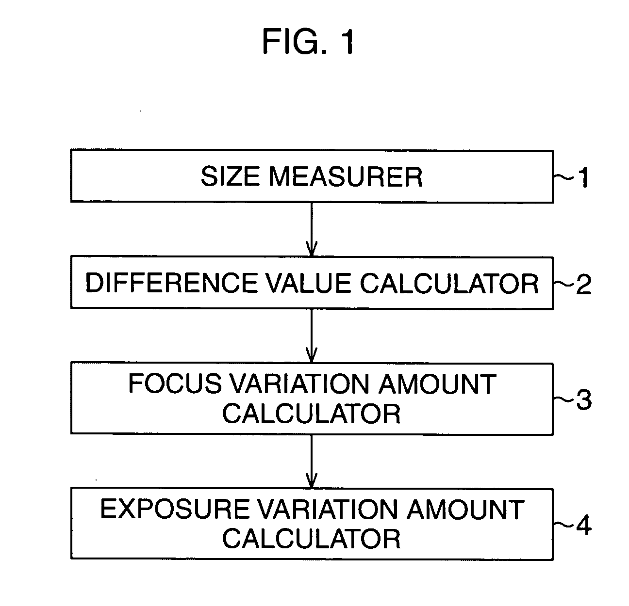
[0037]FIG. 1 is a block diagram schematically showing a structure of the exposure measurement apparatus according to the present embodiment. The exposure measurement apparatus is structured to include a size measurer 1 for measuring respective sizes of at least a pair of transferred patterns having mutually different optimal focus positions out of a plurality of transferred patterns formed by being transferred for example onto a silicon wafer being a transfer object, a difference value calculator 2 for obtaining a difference value between the size of one transferred pattern and the size of the other transferred pattern, and a focus variation amount calculator 3 for calculating a focus error amount of the silicon wafer when the pattern is transferred...

first example

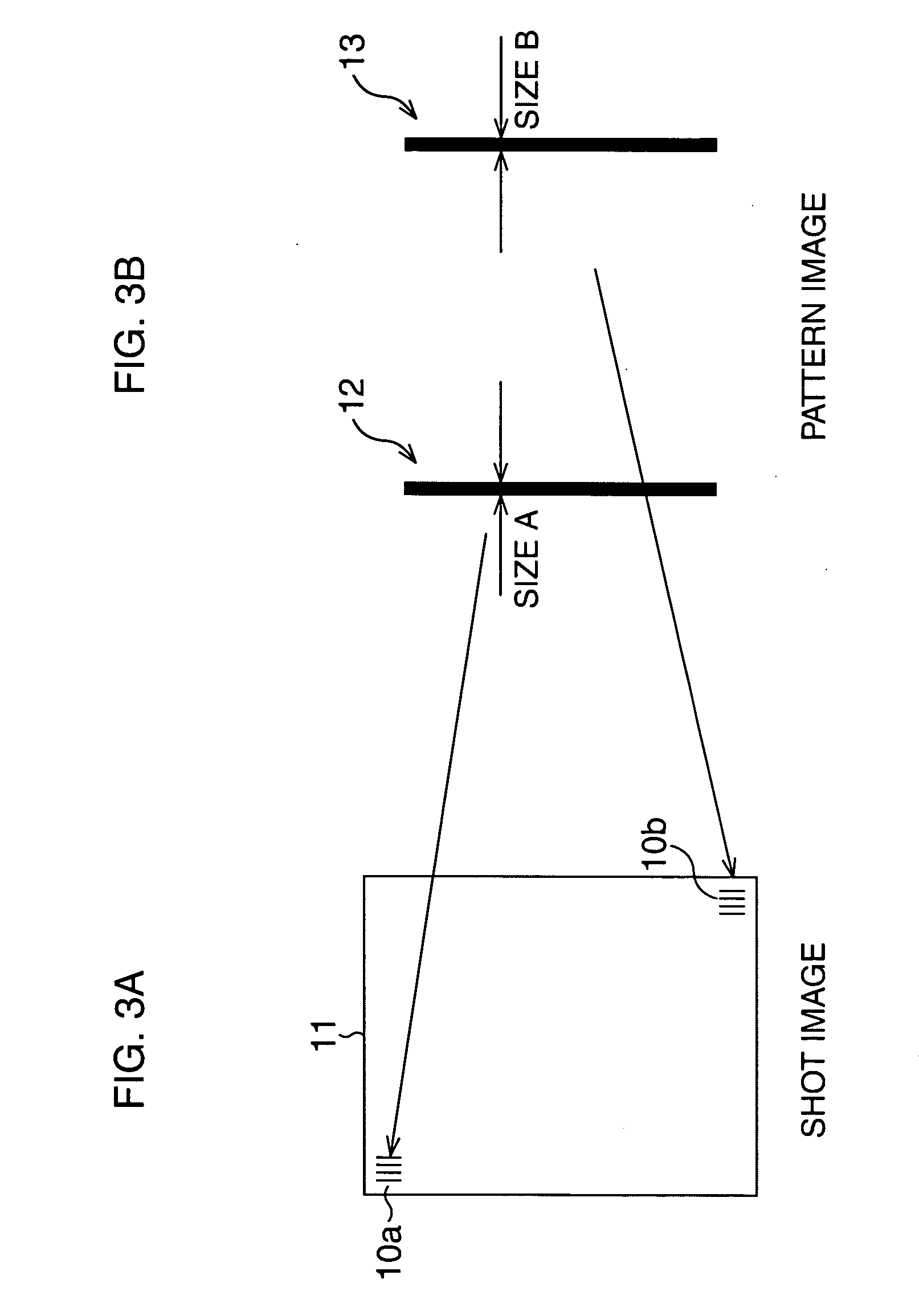
[0048]FIGS. 6A and 6B are plan views showing a pattern of a first example according to the present embodiment. FIG. 6A shows a shot image when the patterns are exposed, and FIG. 6B shows a pattern image transferred, respectively.

[0049] In this example, height of images 20a to 20d are inserted into four corners of an exposure site (one shot) 21 being one exposure site as shown in FIG. 6A. A resist pattern corresponding to each height of image is to have a kinked line shape, here, an L-shaped pattern 22 being in a substantially L shape as shown in FIG. 6B, and the mutually crossing respective straight line patterns of the L-shaped pattern 22 constitute a pair of transferred patterns 23, 24.

[0050] Generally, an aligner has aberration of a lens in the nature thereof. The aberration is designed to come to be small as much as possible, but it is impossible to bring it to completely zero (0). For instance, in the case of the lens having astigmatism, a difference appears at an optimal foc...

second example

[0052]FIGS. 7A and 7B are plan views showing a pattern of a second example according to the present embodiment, in which FIG. 7A shows a shot image when the patterns are exposed, and FIG. 6B shows a pattern image transferred, respectively.

[0053] In this example, height of images 30a to 30d are inserted into four corners of an exposure site (one shot) 31 being one exposure site as shown in FIG. 7A. A resist pattern corresponding to each height of image is to have a kinked line shape, here, a V-shaped pattern 32 being in a substantially V shape as shown in FIG. 7B, and the mutually crossing respective straight line patterns of the V-shaped pattern 32 constitute a pair of transferred patterns 33, 34. Specifically, the V-shaped pattern 32 of this embodiment is the L-shaped pattern 22 of previously-described example 1 turned at an angle of 45 degrees on the document.

[0054] The V-shaped pattern 32 allows reading out the focus error amount and the exposure error amount from the pair of t...


PUM


Abstract

An exposure measurement apparatus is configured by including a size measurer measuring respective sizes of at least a pair of transferred patterns having mutually different optimal focus positions out of a plurality of transferred patterns formed by being transferred onto a transfer object, a difference value calculator obtaining a difference value between the size of one transferred pattern and the size of the other transferred pattern, a focus variation amount calculator calculating a focus variation amount of the transfer object using the difference value, and an exposure variation amount calculator calculating an exposure error amount of a wafer.

Description

CROSS-REFERENCE TO RELATED APPLICATIONS [0001] This application is based upon and claims the benefit of priority from the prior Japanese Patent Application No. 2004-177098, filed on Jun. 15, 2004, the entire contents of which are incorporated herein by reference. BACKGROUND OF THE INVENTION [0002] 1. Field of the Invention [0003] The present invention relates to a measurement method and an apparatus for measuring a focus error amount and so forth when a pattern is exposed in a lithographic process for manufacturing a semiconductor device and a display device such as a liquid crystal, and a semiconductor device manufacturing method. [0004] 2. Description of the Related Art [0005] Recently, along with highly improving density of a semiconductor element, a pattern formed by a lithography technique shows progress in microfabrication. The finer the pattern becomes, the smaller the requirement for size uniformity becomes. As one major cause that deteriorates the size uniformity, a focus v...

Claims


Application Information

Patent Timeline
IPC IPC(8): G03C5/00G03F1/00G03F7/20G06K9/00H01L21/027
CPCG03F7/70641
Inventor YAMAMOTO, TOMOHIKO
Owner FUJITSU SEMICON LTD
Why Eureka
Try Eureka