Organic semiconductor element and manufacturing method thereof

Inactive Publication Date: 2005-12-22
KK TOSHIBA
View PDF11 Cites 20 Cited by
  • Summary
  • Abstract
  • Description
  • Claims
  • Application Information

AI Technical Summary

Problems solved by technology

Among these printing methods, the ink jetting method is capable of direct drawing without using a mask or the like and is effective also for miniaturization of an element structure, but has a drawback of low efficiency in manufacturing an organic semiconductor element.
Therefore, manufacturing cost of the organic semiconductor element tends to increase and they are not suitable for fabricating organic semiconductor elements in small quantity and various kinds.
Moreover, the offset printing and the gravure printing have a drawback that the element structure cannot be sufficiently miniaturized.
On the other hand, the low-molecular organic semiconductor materials suc

Method used


Image

  • Organic semiconductor element and manufacturing method thereof
  • Organic semiconductor element and manufacturing method thereof
  • Organic semiconductor element and manufacturing method thereof

Examples


Embodiment Construction

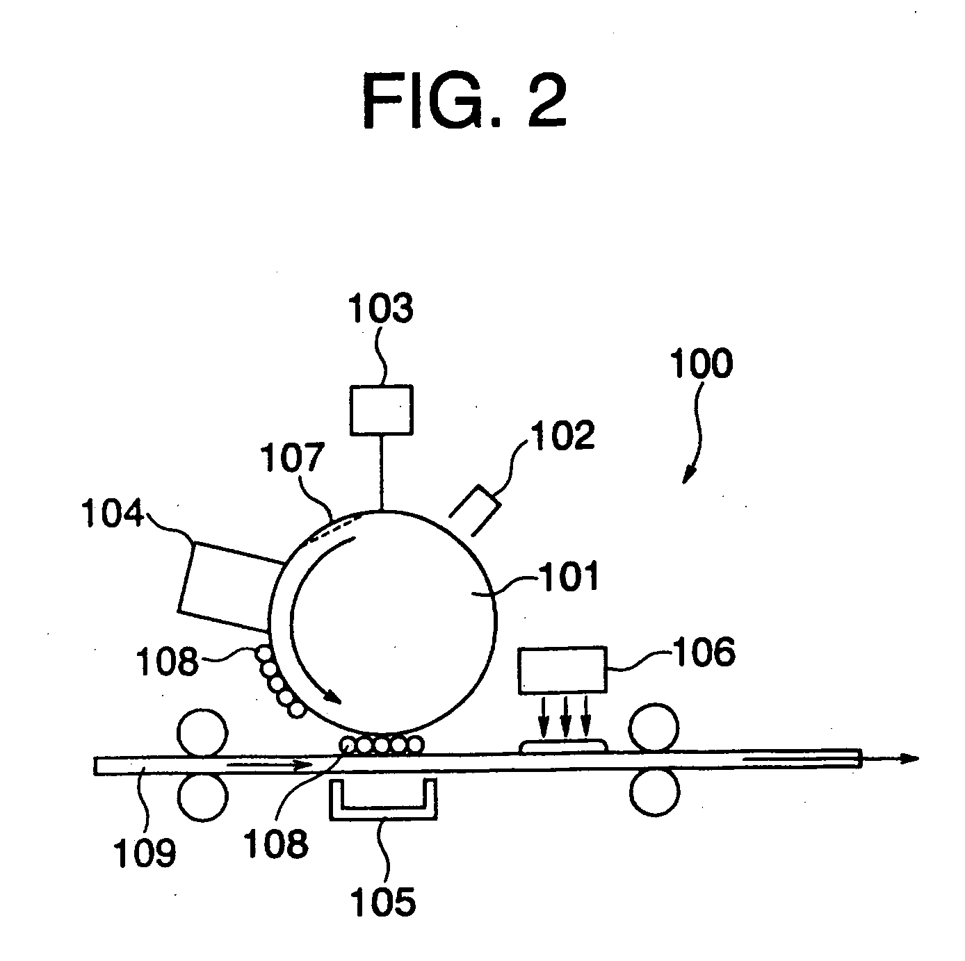
[0022] Hereinafter, embodiments of the present invention will be described with reference to the drawings. It should be noted that, though the embodiments of the present invention will be described based on the drawings, these drawings are provided only for an illustrative purpose and in no way are to limit the present invention.

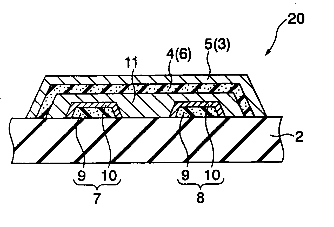
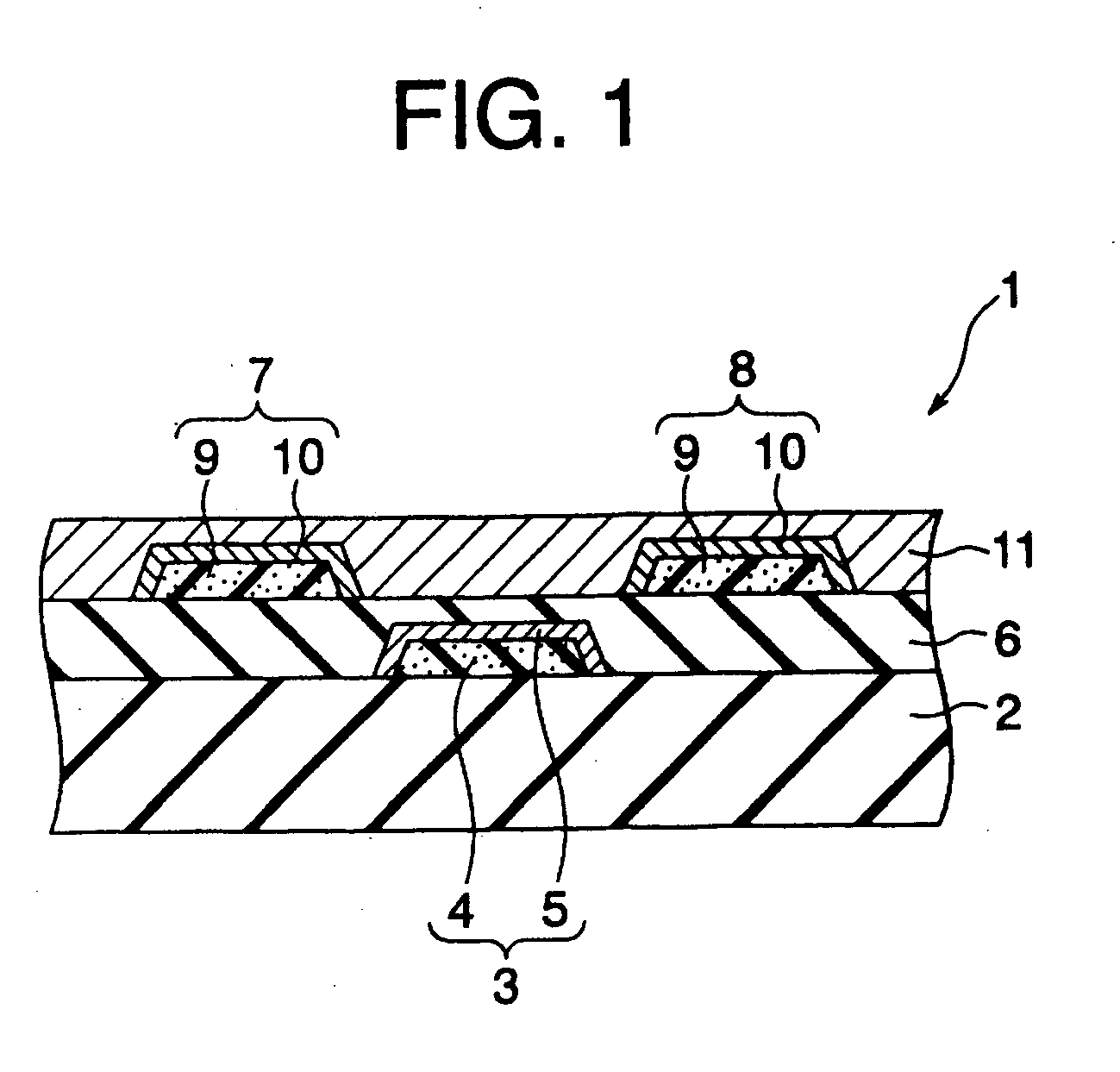
[0023]FIG. 1 is a sectional view showing a rough structure of an organic semiconductor element according to a first embodiment of the present invention. An organic semiconductor element 1 shown in the drawing has a substrate 2 made of, for example, an insulation resin. In particular, a flexible resin substrate such as an insulation resin film is effective for making full use of characteristics of the organic semiconductor element 1 and is preferable also from the viewpoint of reducing manufacturing cost, expanding applicable fields, and so on of the organic semiconductor element 1. However, a constituent material of the substrate 2 is not limited to the ins...


PUM


Abstract

An organic semiconductor element comprises an organic semiconductor layer and an electrode supplying an electric current or an electric field to the organic semiconductor layer. The organic semiconductor layer includes a heat fusion layer of organic semiconductor particles. The heat fusion layer of the organic semiconductor particles is formed in such a manner that, for example, the organic semiconductor particles are made to adhere on a layer that is to be a base, by using an electrophotographic method, and thereafter, an adhesion layer of the organic semiconductor particles is heated to fusion bond the organic semiconductor particles. According to such an organic semiconductor element and a manufacturing method thereof, it is possible to enhance element manufacturing efficiency without an advantage of low cost and a miniaturization of an element structure.

Description

CROSS-REFERENCE TO RELATED APPLICATIONS [0001] This application is based upon and claims the benefit of priority from the prior Japanese Patent Application No. 2004-177880, filed on Jun. 16, 2004; the entire contents of which are incorporated herein by reference. BACKGROUND [0002] 1. Field of the Invention [0003] The present invention relates to an organic semiconductor element and a manufacturing method thereof. [0004] 2. Description of the Related Art [0005] In recent years, studies on an organic semiconductor element utilizing an organic semiconductor material for its active layer have been rapidly progressing. As an organic semiconductor element, known is an organic thin film transistor (an organic TFT) of an field effect type in which an organic semiconductor layer is formed, via a gate insulation film, on a gate electrode provided on a resin substrate, and a source electrode and a drain electrode are formed thereon (for example, Japanese Patent Laid-open Application No. 0.2000...

Claims


Application Information

Patent Timeline
IPC IPC(8): H01L29/04H01L29/08H01L29/10H01L31/036H01L35/24H01L51/00H01L51/05
CPCH01L51/0003H01L51/0015H01L51/0545H01L51/0541H01L51/0017H10K71/211H10K71/231H10K71/12H10K10/464H10K10/466
Inventor TAKUBO, CHIAKIAOKI, HIDEOYAMAGUCHI, NAOKO
Owner KK TOSHIBA
Why Eureka
Try Eureka