Methods of patterning a magnetic stack of a magnetic memory cell and structures thereof

a magnetic memory cell and stack technology, applied in the manufacture/treatment of galvano-magnetic devices, semiconductor devices, electrical apparatus, etc., can solve the problems of shortening the device life, achieve the effect of reducing the number of mask levels, reducing device failures, and improving yield

Active Publication Date: 2005-12-22
INFINEON TECH AG +1
View PDF22 Cites 40 Cited by
  • Summary
  • Abstract
  • Description
  • Claims
  • Application Information

AI Technical Summary

Benefits of technology

[0008] Embodiments of the present invention provide novel methods of patterning magnetic memory cells of a FET MRAM device. Embodiments of the present invention provide methods of patterning MTJ's of magnetic memory devices that prevent the formation of metal fences on the sidewalls of various material layers of the devices by using a sidewall spacer hard mask formed over sidewalls of a first hard mask and top magnetic layers to pattern the underlying material layers of the magnetic stack.
[0011] Advantages of preferred embodiments of the present invention include providing methods of patterning MTJ's of MRAM devices, and structures thereof, that prevent shorting between the MTJ's and the conductive lines used to access the MTJ's, resulting in reduced device failures and improved yields. Few or no additional masks are required, and in one embodiment, the number of mask levels can be reduced. Because an anisotropic etch is used to form the sidewall spacers that are used as a second hard mask, no spacer material resides on the top surface of the hard mask over the second magnetic layer, and no mask is required to form the novel sidewall spacer hard mask. This is advantageous because after the sidewall spacer hard mask formation, the device can be electrically tested in the middle of the manufacturing process, by contacting the first hard mask formed over the MTJ top electrode (or second magnetic material layer), which is conductive. Embodiments of the present invention provide the ability to manufacture MTJ's having a smaller cell size, which results in the ability to place the MTJ's closer together, resulting either in a smaller memory array, or in the ability to put more cells in the same square unit of chip area.

Problems solved by technology

Because MRAM devices operate differently than traditional memory devices, they introduce design and manufacturing challenges.
For example, the magnetic material layers and other metal layers that form the magnetic memory cells of an MRAM device are difficult to etch and have a high sputter component, resulting in re-deposition of conductive material in undesired locations, which can short out the devices.

Method used


Image

  • Methods of patterning a magnetic stack of a magnetic memory cell and structures thereof
  • Methods of patterning a magnetic stack of a magnetic memory cell and structures thereof
  • Methods of patterning a magnetic stack of a magnetic memory cell and structures thereof

Examples


Embodiment Construction

[0021] The making and using of the presently preferred embodiments are discussed in detail below. It should be appreciated, however, that the present invention provides many applicable inventive concepts that can be embodied in a wide variety of specific contexts. The specific embodiments discussed are merely illustrative of specific ways to make and use the invention, and do not limit the scope of the invention.

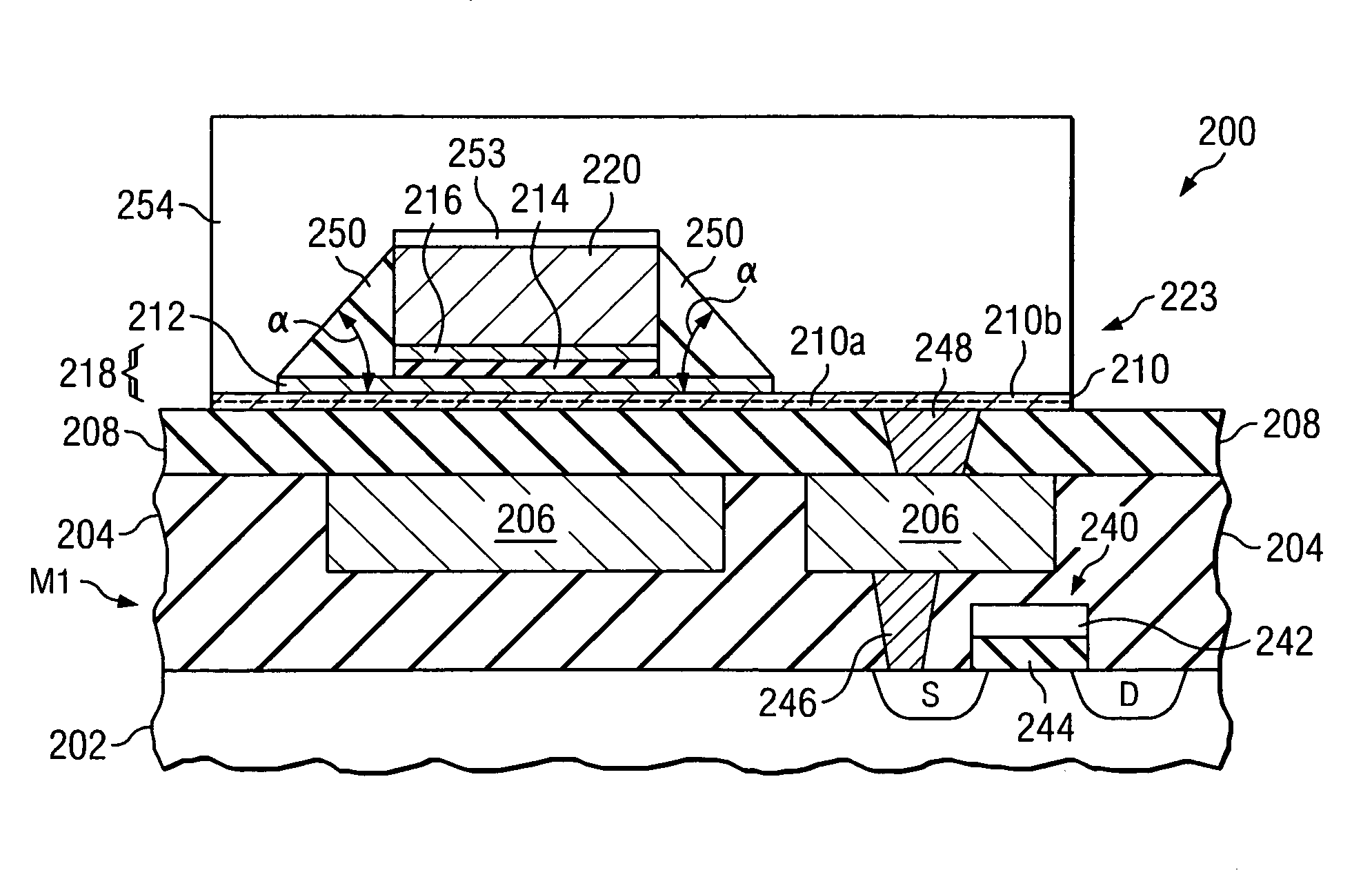
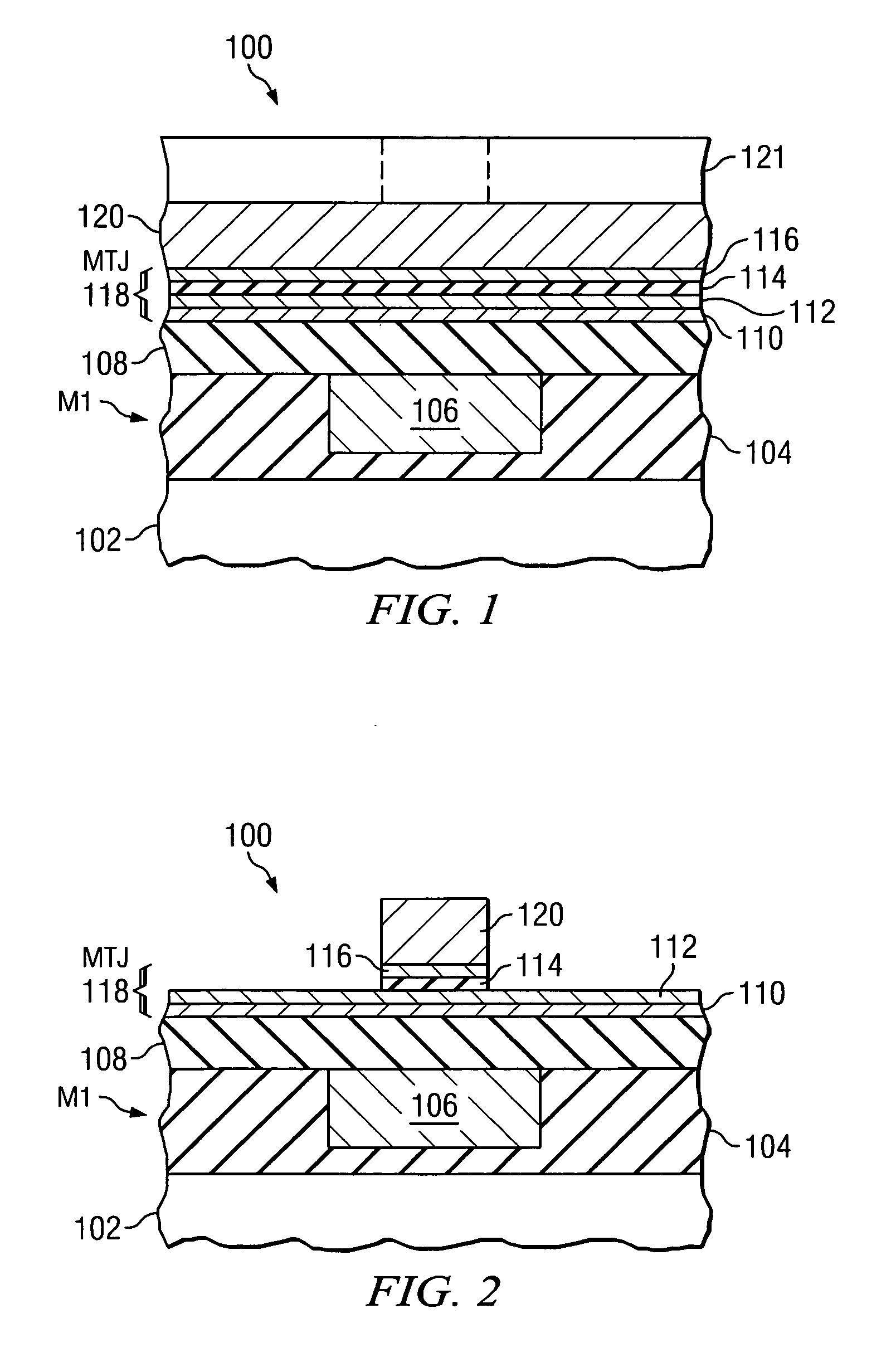
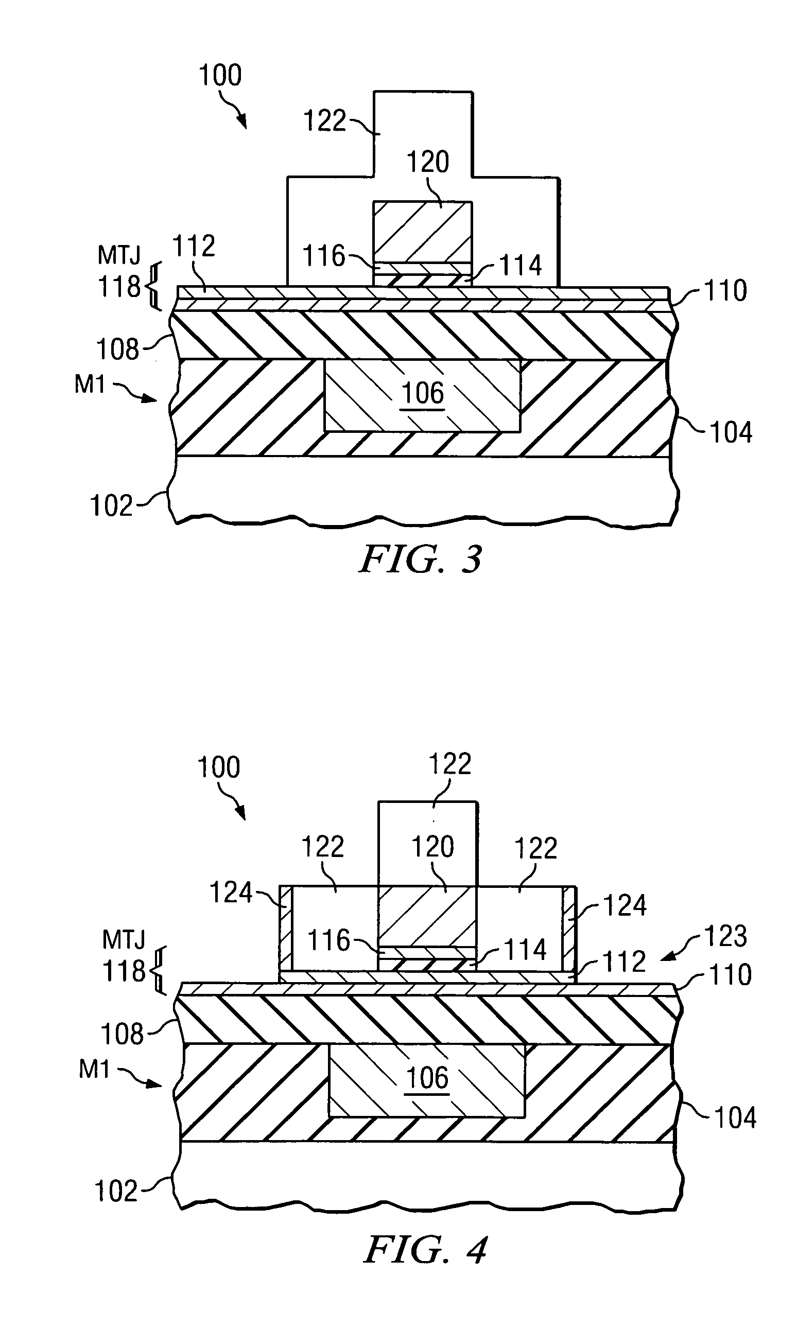
[0022] The present invention will be described with respect to preferred embodiments in a specific context, namely an MRAM device. Embodiments of the present invention may also be applied, however, to other magnetic memory cell designs and magnetic semiconductor device applications. Only one MTJ is shown in each of the figures. However, a plurality of MTJ's may be simultaneously formed using the manufacturing processes described herein. For example, an array of MTJ's may be patterned using embodiments of the present invention. The present invention is particularly beneficia...


PUM

PropertyMeasurementUnit
widthaaaaaaaaaa
angleaaaaaaaaaa
thicknessaaaaaaaaaa

Abstract

Methods of patterning a magnetic stack of a magnetic memory cell and structures thereof. At least the top magnetic material layer of a magnetic stack is patterned using a hard mask, and a conformal insulating material is deposited over the patterned top magnetic material layer and hard mask. The conformal insulating material is anisotropically etched to remove the conformal insulating material from horizontal surfaces of the device, leaving portions of the conformal insulating material over vertical sidewalls of at least the patterned top magnetic material layer and the hard mask. The remaining conformal insulating material comprises a sidewall spacer hard mask that is used as a mask to pattern the remaining material layers of the magnetic stack. The sidewall spacer hard mask may be left remaining in the magnetic memory cell structure.

Description

CROSS-REFERENCE TO RELATED APPLICATIONS [0001] This application relates to the following co-pending and commonly assigned patent application: Ser. No. ______, filed on Jun. 15, 2004, attorney docket number 2003 P 52580 US, entitled “Mask Schemes for Patterning Magnetic Tunnel Junctions,” which application is hereby incorporated herein by reference.TECHNICAL FIELD [0002] The present invention relates generally to the fabrication of semiconductor devices, and more particularly to the fabrication of magnetic memory devices. BACKGROUND [0003] Semiconductors are used in integrated circuits for electronic applications, including radios, televisions, cell phones, and personal computing devices, as examples. One type of semiconductor device is a semiconductor storage device, such as a dynamic random access memory (DRAM) and flash memory, which use a charge to store information. [0004] A recent development in semiconductor memory devices involves spin electronics, which combines semiconducto...

Claims


Application Information

Patent Timeline
Patent Type & Authority Applications(United States)
IPC IPC(8): H01L21/335H01L27/22H01L29/76H01L43/12
CPCH01L43/12H01L27/228H10B61/22H10N50/01
Inventor KASKO, IHARKANAKASABAPATHY, SIVANANDHA K.COSTRINI, GREGORY
Owner INFINEON TECH AG
Why Eureka
Try Eureka