
Mura defect inspection mask, apparatus and method of inspecting the mura defect, and method of producing a photomask

Inactive Publication Date: 2005-12-22
HOYA CORP
View PDF19 Cites 13 Cited by
  • Summary
  • Abstract
  • Description
  • Claims
  • Application Information

AI Technical Summary

Benefits of technology

[0020] The present invention has been achieved in view of the above-discussed circumstances. One of objects of the present invention is to provide a method of inspecting an mura defect in which an mura defect occurring in a repetitive pattern of a member to be inspected can be evaluated qualitatively and quantitatively, and the mura defect can be accurately detected.
[0021] It is one of other objects of the present invention to provide an apparatus for inspecting the mura defect which can evaluate qualitatively and quantitatively the mura defect occurring in the repetitive pattern of the member to be inspected, and accurately detect the mura defect.
[0022] It is one of further objects of the present invention to provide a method of producing a photomask which enables the mura defect occurring in a repetitive pattern of a photomask to be evaluated qualitatively and quantitatively, and detected accurately.
[0052] According to the present invention, plural pseudo mura defects of the mura defect inspection mask are detected, whereby the detection sensitivity is ascertained or calibrated. Therefore, the apparatus for inspecting the mura defect is surely set to a detection sensitivity which is set in a mura defect inspection mask for each of pseudo mura defect, and at which plural different-intensity pseudo mura defects can be detected. Consequently, the mura defect occurring in a repetitive pattern in a member to be inspected or a photomask can be accurately detected.

Problems solved by technology

When any of the above-described writing systems is employed, writing joints exist due to the beam scan width or the beam diameter, and there arises a problem in that an error due to a writing failure such as a butting error occurring in such joints is periodically caused in each of the writing units.
Even when each of the errors has a size which is so small as to be invisible in micro scale (for example, several tens of nm), the errors result in a continuous linear error become to be visible.
As a result, a mura defect such as mura in sensitivity or that in display occurs to cause a problem in that the performance of the device is lowered.
However, these inspections are conducted for inspecting local defects on a photomask, and hence hardly detect a defect such as the mura defect or a defect which is recognized only in a wide area on the photomask.
Because of this reason and the like, the mura defect of the photomask cannot be accurately detected.
As a result, there is a problem in that the yield of devices is lowered.
In a device produced with using the photomask, it is considered that the mura defect of the device is caused not only by the photomask but also by other reasons such as stitching exposure of the photomask.
In the apparatus for inspecting the mura defect disclosed in the JP-A-10-300447, it is difficult to identify the cause of a detected mura defect.
Furthermore, there are various kinds of mura defects in which shapes and regularities are different depending on, for example, the cause of occurrence.
However, the apparatus for inspecting the mura defect disclosed the JP-A-10-300447 cannot accurately detect plural kinds of mura defects which are required to be inspected.
However, the apparatus cannot qualitatively evaluate the mura defect, and, for example, cannot differentiate the mura defect which requires an inspection from that which does not require an inspection, or quantitatively evaluate an mura defect on the basis of the intensity of the defect.

Method used


Image

  • Mura defect inspection mask, apparatus and method of inspecting the mura defect, and method of producing a photomask
  • Mura defect inspection mask, apparatus and method of inspecting the mura defect, and method of producing a photomask
  • Mura defect inspection mask, apparatus and method of inspecting the mura defect, and method of producing a photomask

Examples


Embodiment Construction

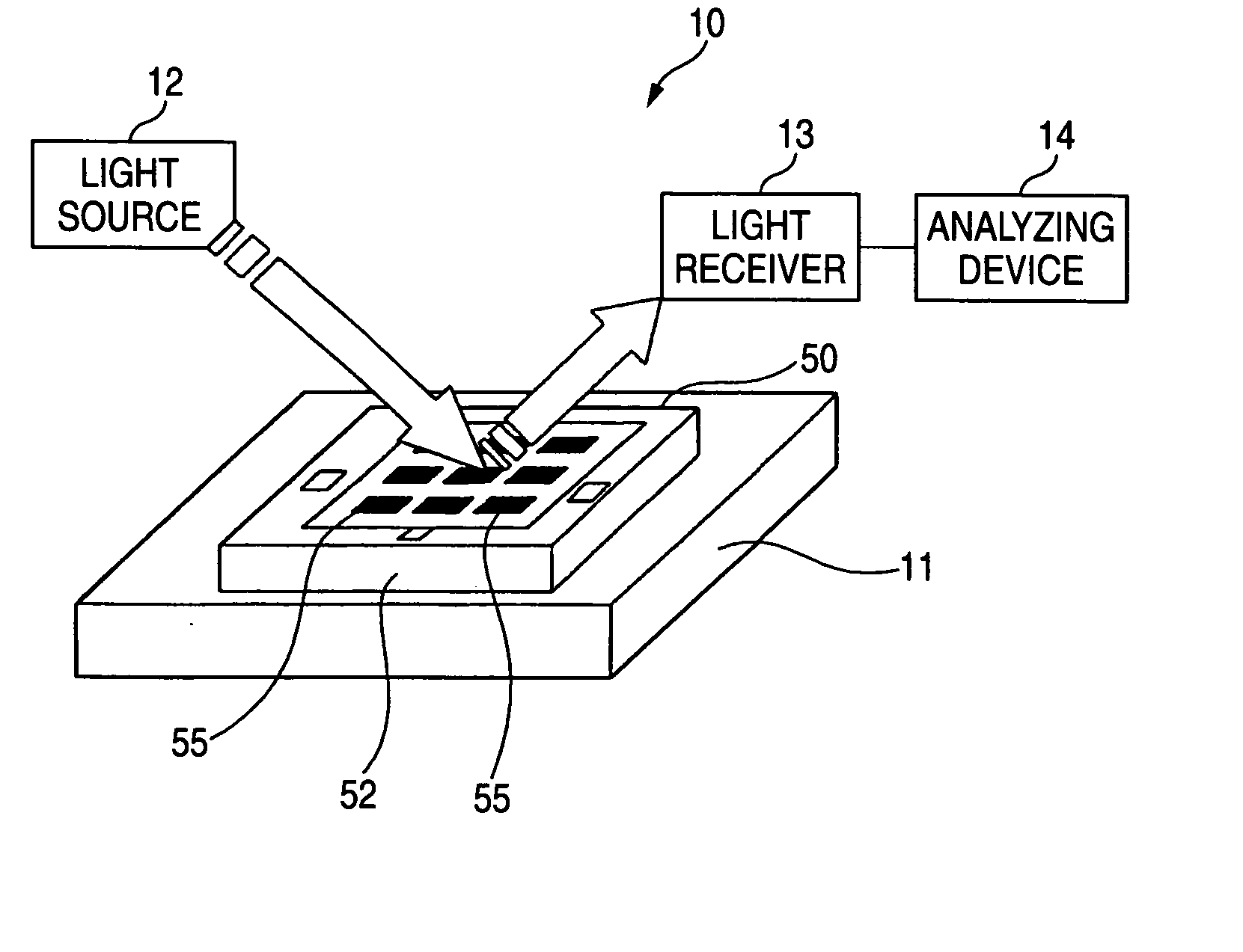
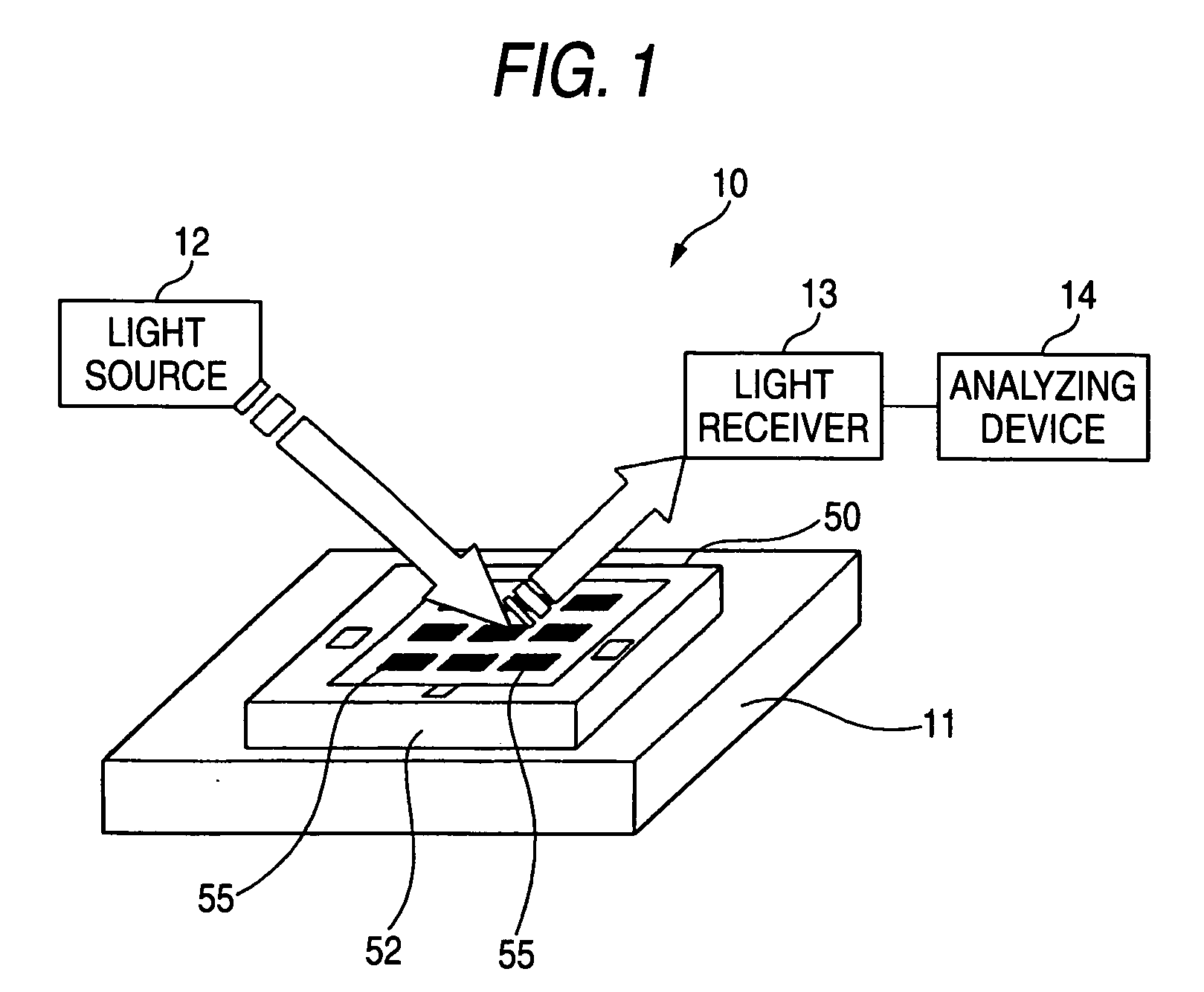
[0062] Hereinafter, the best mode for carrying out the present invention will be described with reference to the accompanying writings.

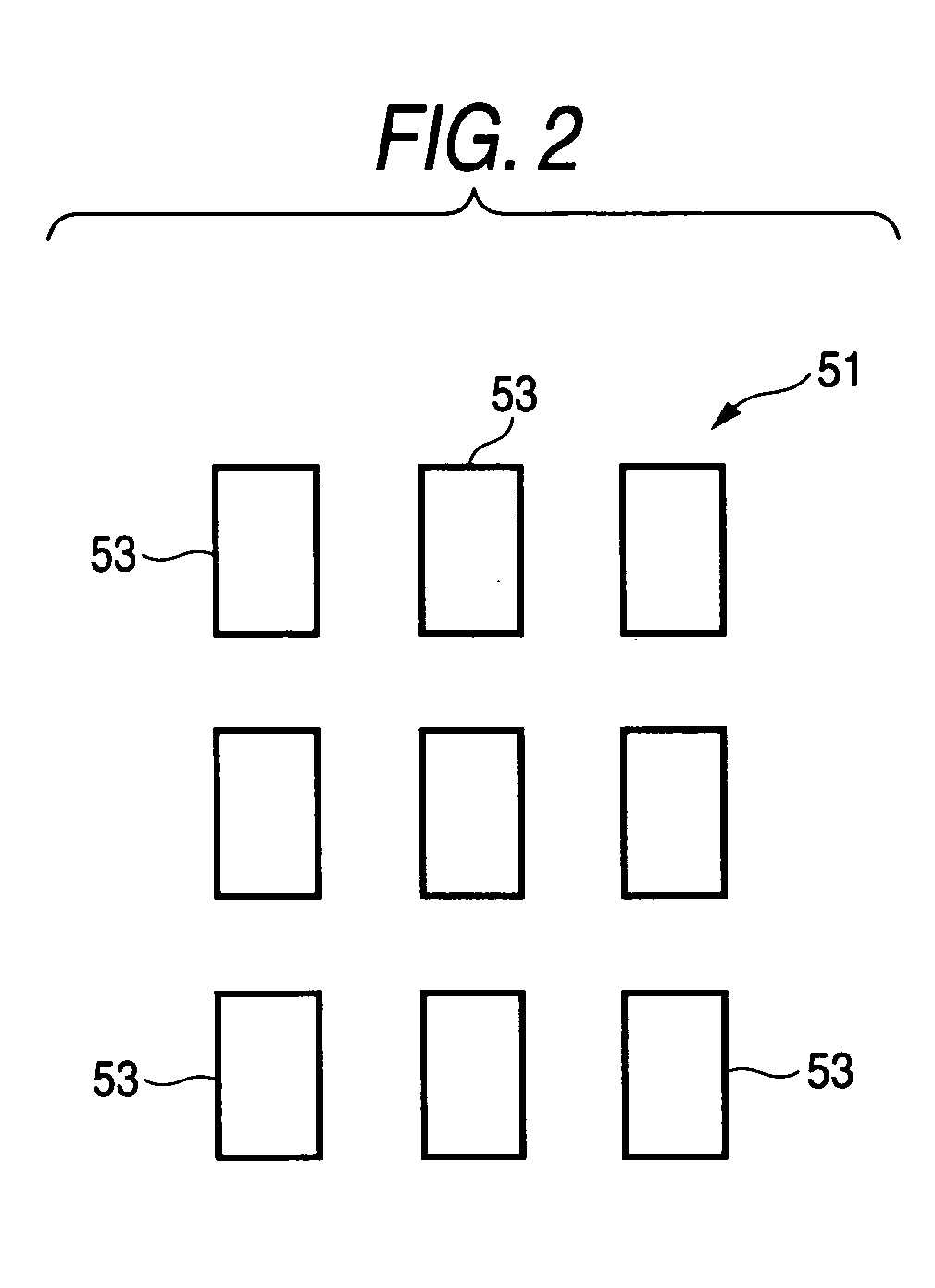
[0063]FIG. 1 is a perspective view showing the configuration of an embodiment of an apparatus for inspecting an mura defect according to the present invention, and FIG. 2 is a plan view showing a repetitive pattern in a chip of a photomask in FIG. 1.

[0064] The mura defect inspecting apparatus 10 shown in FIG. 1 detects the mura defect occurring in a repetitive pattern 51 (FIG. 2) formed on the surface of a photomask 50 which is a member to be inspected, and is configured by a stage 11, a light source 12, a light receiver 13, and an analyzing device 14. The photomask 50 is an exposure mask for producing a image device.

[0065] The image device is a device in which many pixel patterns are finally subjected to image processing or image display. Examples of such a device are an imaging device and a display device. Typical examples of the imaging device ...


PUM


Abstract

Plural repetitive patterns 61 are formed on a transparent substrate 62 in the unit of a chip 65. Each of the repetitive patterns has plural pseudo mura defects 66 to which intensities of mura defects occurring in a predetermined repetitive pattern are allocated with being stepwise changed, for respective kinds of the mura defects. The mura defects are a CD Mura based on an abnormality in critical dimension of unit patterns 63 in the repetitive patterns, a Pitch Mura based on an abnormality in interval of the repetitive patterns, a Butting Mura-based on a positional displacement of the repetitive patterns, and a Defect mura based on a pattern defect of unit patterns in the repetitive patterns.

Description

[0001] The present invention claims foreign priority to Japanese patent application no. P.2004-159765, filed on May 28, 2004, the contents of which is incorporated herein by reference. BACKGROUND OF THE INVENTION [0002] 1. Field of the Invention [0003] The present invention relates to a method of inspecting an mura defect, an apparatus for inspecting an mura defect, and a method of producing a photomask. [0004] 2. Description of the Related Art [0005] A photomask used in pattern formation in a process of producing a semiconductor device, an imaging device, or a display device has a configuration in which a opaque film made of chromium or the like is partly removed away to be formed into a desired pattern on a transparent substrate such as a glass plate. [0006] The photomask is produced in the following method. The opaque film is formed on the transparent substrate, and a resist film is formed on the opaque film. Then, a predetermined pattern is exposed onto the resist film by conduc...

Claims


Application Information

Patent Timeline
IPC IPC(8): G01B11/30G01M11/00G01N21/88G01N21/956G03F1/84H01L21/027
CPCG01N21/956G03F1/44G03F7/7065H01L22/12
Inventor MURAI, MAKOTO
Owner HOYA CORP
Features
  • Generate Ideas
  • Intellectual Property
  • Life Sciences
  • Materials
  • Tech Scout
  • Unparalleled Data Quality
  • Higher Quality Content
  • 60% Fewer Hallucinations
Learn More