Real time testing using on die termination (ODT) circuit

a real-time testing and circuit technology, applied in the field of electronic devices, can solve the problems of jitter on output signals, significantly deteriorating output signal quality, negative affecting chip performance during routine high-speed data transfer operations, etc., and achieve the effect of increasing the speed of data output paths and maximizing chip real estate utilization

Inactive Publication Date: 2005-12-22
MICRON TECH INC
View PDF23 Cites 28 Cited by
  • Summary
  • Abstract
  • Description
  • Claims
  • Application Information

AI Technical Summary

Benefits of technology

[0022] According to a system and method of the present disclosure an electronic device, such as a memory chip, is operated in a test mode using the device's built-in ODT circuit. One or more test mode related signals, which include on-die signals and other relevant information, may be transferred from the integrated circuit of the electronic device to an external processor using the device's ODT circuit instead of the output data signal driver circuit. Therefore, no capacitive loading of output drivers occurs during test mode operations. Thus the speed of the output data path (i.e., the circuit path propagating non-test mode related signals from the electronic device to other external units in the system) is not affected by test mode operations, allowing a system designer to increase the speed of the data output path as much as desired. Also, the use of a minimal number of logic gates along with the existing ODT circuits to perform transmission of test mode related signals substantially maximizes chip real estate utilization without waste.

Problems solved by technology

Also, such “loading” of output drivers 38 by testing related logic circuitry negatively affects chip performance during routine high speed data transfer operations (e.g., typical memory read / write operations during run time).
For example, more gates added to output drivers 38 for testing related circuitry may not only result in additional output delays, but may also cause jitter on output signals and may significantly deteriorate quality of output signals.
The on chip placement of such extra output drivers would also result in unnecessary waste of chip real estate.

Method used


Image

  • Real time testing using on die termination (ODT) circuit
  • Real time testing using on die termination (ODT) circuit
  • Real time testing using on die termination (ODT) circuit

Examples


Embodiment Construction

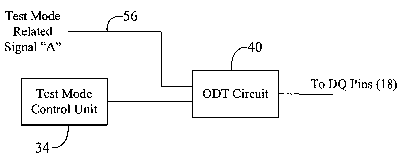
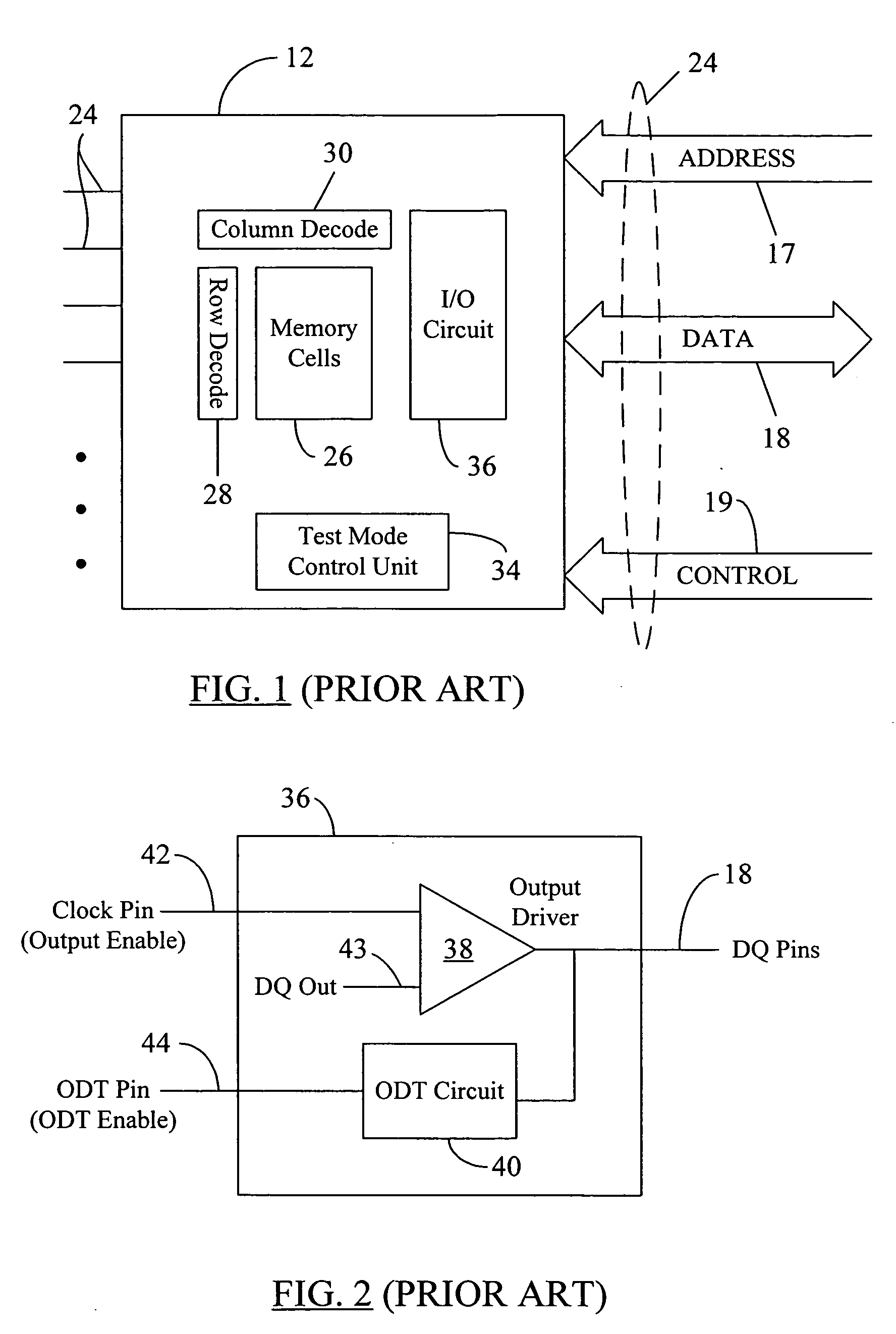
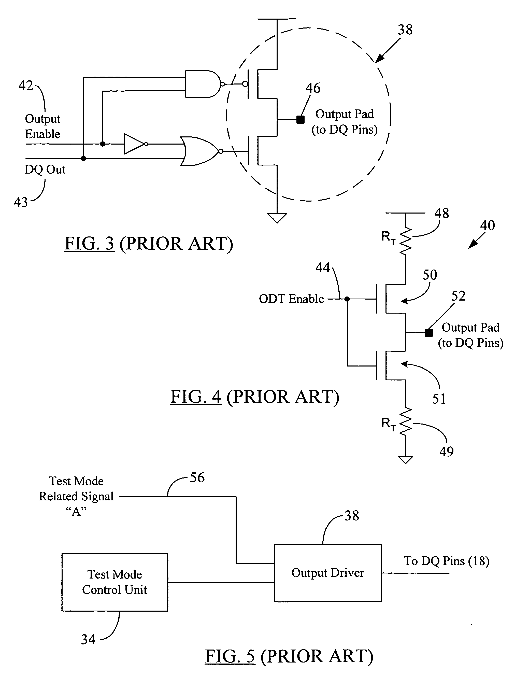
[0033] Reference will now be made in detail to some embodiments of the present disclosure, examples of which are illustrated in the accompanying drawings. It is to be understood that the figures and descriptions of the present disclosure included herein illustrate and describe elements that are of particular relevance to the present disclosure, while eliminating, for the sake of clarity, other elements found in typical solid-state electronic devices, memories or memory-based systems. It is noted at the outset that the terms “connected”, “connecting,”“electrically connected,” etc., are used interchangeably herein to generally refer to the condition of being electrically connected. It is further noted that various block diagrams and circuit diagrams shown and discussed herein employ logic circuits that implement positive logic, i.e., a high value on a signal is treated as a logic “1” whereas a low value is treated as a logic “0.” However, any of the circuit discussed herein may be eas...


PUM


Abstract

A system and method to operate an electronic device, such as a memory chip, in a test mode using the device's built-in ODT (on die termination) circuit is disclosed. One or more test mode related signals, which include on-die signals and other relevant information, may be transferred from the integrated circuit of the electronic device to an external processor using the device's ODT circuit instead of the output data signal driver circuit. Therefore, no capacitive loading of output drivers occurs during test mode operations. Thus the speed of the output data path (i.e., the circuit path propagating non-test mode related signals from the electronic device to other external units in the system) is not affected by test mode operations, allowing a system designer to increase the speed of the data output path as much as desired. Further, deterioration in the quality of signals output from the output drivers is also avoided. Also, the use of a minimal number of logic gates along with the existing ODT circuits to perform transmission of test mode related signals substantially maximizes chip real estate utilization without waste. Because of the rules governing abstracts, this abstract should not be used to construe the claims.

Description

BACKGROUND [0001] 1. Field of the Disclosure [0002] The present disclosure generally relates to testing of electronic devices and, more particularly, to a system and method to test semiconductor memory chips. [0003] 2. Brief Description of Related Art [0004] Memory devices are widely used in many electronic products and computers to store data. A memory device is a semiconductor electronic device that includes a number of memory cells, each cell storing one bit of data. The data stored in the memory cells can be read during a read operation. FIG. 1 is a simplified block diagram showing a memory chip or memory device 12. The memory chip 12 may be part of a DIMM (dual in-line memory module) or a PCB (printed circuit board) containing many such memory chips (not shown in FIG. 1). The memory chip 12 may include a plurality of pins 24 located outside of chip 12 for electrically connecting the chip 12 to other system devices. Some of those pins 24 may constitute memory address pins or add...

Claims


Application Information

Patent Timeline
Patent Type & Authority Applications(United States)
IPC IPC(8): G06F11/00G11C29/48
CPCG11C29/48G11C29/1201
Inventor STAVE, ERIC J.
Owner MICRON TECH INC
Why Eureka
Try Eureka